Infrared detector chip for increasing capacitance density

An infrared detector and capacitance density technology, applied in the field of infrared detectors, can solve the problems of reduced capacitance area, poor matching of readout circuits, and small capacitance density, so as to increase capacitance density, improve performance matching, and capacitance density. Enhanced effect

Active Publication Date: 2019-06-11
SHANGHAI INTEGRATED CIRCUIT RES & DEV CENT
View PDF5 Cites 2 Cited by
  • Summary
  • Abstract
  • Description
  • Claims
  • Application Information

AI Technical Summary

Problems solved by technology

A large number of capacitor structures will be used in the infrared detector reading circuit, including AD / DA, integrator, sample / hold and other modules, which will need to use larger capacitors. At this time, the capacitor area and its matching gradually become the product and process design. Especially when the chip size is close to the maximum size of a single exposure in lithography, in order not to exceed this size and the overall cost considerations, a compromise has to be made in the selection of the capacitance area. Reducing the capacitance area will easily lead to a decrease in chip performance. decline
[0003] Existing infrared detector chips include a pixel array and readout circuits located at both ends of the pixel array, as shown in the attached figure 1 As shown, the pixel array includes pixel units 1 in M ​​rows and N columns, and each column of pixel units corresponds to a readout circuit, which includes a capacitor unit 2. With the improvement of chip integration, the area of ​​a single pixel unit also increases. Smaller and smaller, so that the area of ​​the capacitor unit corresponding to each column is also smaller and smaller. The reduction in the area of ​​the capacitor unit, on the one hand, makes the size of the pattern smaller, resulting in a large error in the size of the pattern after photolithography and etching, causing the row The matching between the capacitance and the readout circuit becomes worse; on the other hand, the reduction of the capacitance area also reduces the capacitance density in the chip, so that the detection signal in the infrared detector cannot be read out in time and effectively, which affects the detection device performance
Capacitor units in the prior art have the disadvantage of small capacitance density in addition to their small area. The structures forming capacitors in the prior art are all formed by single-layer metal and through-hole connections, and the through-holes are in the horizontal section. Point structure, due to the small relative area between adjacent through holes, the capacitance value formed by it is also small, which cannot make full use of the limited capacitance area

Method used


Image

  • Infrared detector chip for increasing capacitance density
  • Infrared detector chip for increasing capacitance density
  • Infrared detector chip for increasing capacitance density

Examples


Embodiment 1

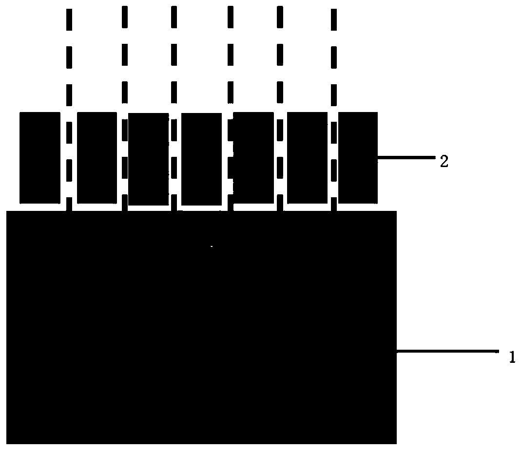
[0029] as attached figure 2 As shown, the purpose of the infrared detector chip provided by the present invention is to increase the area of ​​the capacitor unit, thereby improving the matching between the capacitor units corresponding to different columns and the readout circuits. In this embodiment, the infrared detector chip includes a pixel array 1 and a capacitor array required by the readout circuit. The pixel array 1 includes pixel units of M rows and N columns, and the capacitor array includes capacitor units 2 of 2 rows and N / 2 columns. , wherein the width of the capacitor unit is the sum of the widths of the two pixel units, and the sum of the widths of the two pixel units includes the sum of the two pixel units and their gaps; and the capacitor array is located on the upper side of the detector chip, in the vertical In the direction, the two capacitor units are arranged in parallel and keep the same width as the two pixel units below them. The uppermost side of th...

Embodiment 2

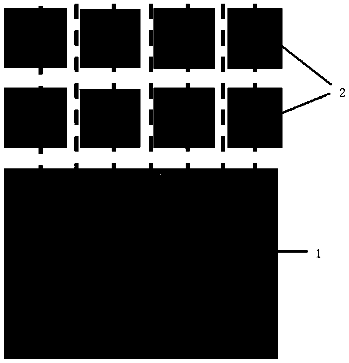
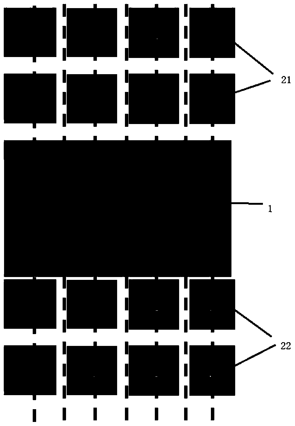
[0033] With the increase of pixel units in the pixel array, if the readout circuit is still distributed on one side of the pixel array, during the signal transmission process of the pixel units in each column, the pixel unit far away from the readout circuit reaches the gap between the capacitor units The parasitic effect is much different from the parasitic effect between the pixel unit close to the readout circuit and the capacitor unit, and as the size of a single pixel unit becomes smaller, it becomes more and more difficult to reduce the parasitic effect by increasing the line width. Therefore, the present invention The capacitor unit of each row of pixel units is split into the upper and lower sides of the pixel array, and the matching between the pixel unit and the capacitor unit is ensured as much as possible.

[0034] The capacitor unit in the present invention includes an upper capacitor array and a lower capacitor array, the upper capacitor array is located above the...

Embodiment 3

[0043] The areas of the metal layer and the through-hole layer in the adjacent metal sub-module and the through-hole sub-module are different on the horizontal section. One correspondence, also may not correspond.

[0044] Please refer to the attached Figure 5 , when the horizontal cross-sectional area of ​​the metal layer 51 is larger than the horizontal cross-sectional area of ​​the via layer 52, the horizontal capacitor 7 can be formed through the dislocation connection of the via layer to the metal layer. Horizontal capacitance can exist between two adjacent metal sub-modules, and can exist between the bottom metal sub-module and the polysilicon module, as shown in the attached Figure 5 shown. Among them, in order to form a horizontal capacitor between metal layers, the following three requirements need to be met: first, the metal layers in adjacent metal sub-modules are opposite in the vertical direction; second, the two opposite metal layers If they are not connecte...


PUM


Abstract

The present invention discloses an infrared detector chip for increasing capacitance density, comprising a pixel array and a capacitor array required for a readout circuit. The capacitor array is positioned above and/or below the pixel array. The pixel array comprises M rows and N columns of pixel units. The capacitor array comprises A rows and N/A columns of capacitor units, and each column of pixel units corresponds to one capacitor unit in the capacitor array. The row directions and the column directions of the capacitor array and the pixel array are the same. The length of the capacitor units in the row direction is equal to the length of A pixel units in the row direction. The infrared detector chip for increasing capacitance density provided by the present invention expands the capacitance between single metal layers into multiple layers, thereby increasing capacitance density. Meanwhile, the capacitor units are distributed above and below the array and the width of the capacitorunits is increased, thereby improving the performance matching between column readout circuits and finally enhancing the performance of the entire chip.

Description

technical field [0001] The invention relates to the field of infrared detectors, in particular to an infrared detector chip with increased capacitance density. Background technique [0002] As the infrared detector array becomes larger and larger, even though the area of ​​a single pixel unit is shrinking, the chip area is also increasing with the increase of the area of ​​the pixel array. A large number of capacitor structures will be used in the infrared detector reading circuit, including AD / DA, integrator, sample / hold and other modules, which will need to use larger capacitors. At this time, the capacitor area and its matching gradually become the product and process design. Especially when the chip size is close to the maximum size of a single exposure in lithography, in order not to exceed this size and the overall cost considerations, a compromise has to be made in the selection of the capacitance area. Reducing the capacitance area will easily lead to a decrease in c...

Claims


Application Information

Patent Timeline
Patent Type & Authority Applications(China)
IPC IPC(8): G01J5/34
Inventor 康晓旭
Owner SHANGHAI INTEGRATED CIRCUIT RES & DEV CENT
Why Eureka
Try Eureka