Eureka AIR delivers breakthrough ideas for toughest innovation challenges, trusted by R&D personnel around the world.

A High Speed ​​Sensitive Amplifier Circuit of SRAM Type Memory

A sensitive amplifier and memory technology, which is applied in the direction of static memory, digital memory information, information storage, etc., can solve the problems of affecting the memory reading speed and large input voltage difference, so as to improve the reaction speed and processing ability, and the input voltage difference The effect of reducing the requirements and speeding up the readout speed

Active Publication Date: 2020-10-16
BEIJING MXTRONICS CORP +1
View PDF6 Cites 0 Cited by
  • Summary
  • Abstract
  • Description
  • Claims
  • Application Information

AI Technical Summary

Problems solved by technology

[0004] The sense amplifier of the existing SRAM type memory circuit generally adopts the positive feedback differential voltage sense amplifier and the common latch type sense amplifier circuit, both of which rely on the feedback of the amplifier circuit part to accelerate the response, but both require the minimum distinguishable The input voltage difference is large, and it takes time to form the input voltage difference, which affects the overall read speed of the memory.

Method used


Image

  • A High Speed ​​Sensitive Amplifier Circuit of SRAM Type Memory

Examples


Embodiment Construction

[0023] Below in conjunction with accompanying drawing and concrete implementation the present invention is described in further detail:

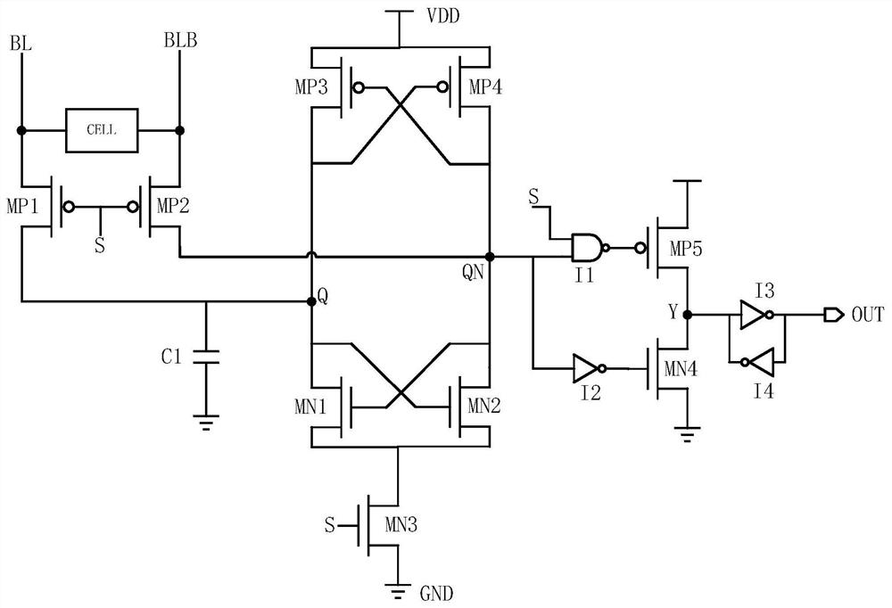
[0024] Such as figure 1 Shown is the circuit structure diagram of the high-speed sense amplifier of the SRAM type memory of the present invention. Consists of: bit line read switch module, latch type amplifier module and output module. The bit line read switch module includes PMOS transistors MP1, MP2, capacitor C1; the latch type amplifier module includes PMOS transistors MP3, MP4, NMOS transistors MN1, MN2, MN3; the read module includes NAND gate I1, inverter I2 -I4, PMOS transistor MP5, NMOS transistor MP4.

[0025] The source terminals of the PMOS transistors MP1 and MP2 in the bit line read switch module are respectively connected to the SRAM unit bit line (CELL) output BL and BLB terminals, and the gate terminals of the PMOS transistors MP1 and MP2 are connected in common, controlled by the read enable input signal S, and the drain ...


PUM


Abstract

The invention relates to a high-speed sensitive amplifier circuit of an SRAM (Static Random Access Memory) type memory, which accelerates the overall response speed of a latch amplifier through positive feedback by virtue of the charge retention characteristic of a capacitor C1 when reading a '1' memory cell, so that the requirement of the amplifier on the input voltage difference is greatly reduced, and the speed of the SRAM type memory for reading the '1' is accelerated; When the '0' storage unit is read, the storage data is read by virtue of the fast pull-up action of the transistor MP5 through the control on the NAND gate I1 by the hopping of the read enable signal S, so that the requirement on the input voltage difference is greatly reduced, the reading speed of the sense amplifier isaccelerated, and the speed of the SRAM for reading the '0' is accelerated. The requirement of the sensitive amplifier for the input voltage difference is reduced, and the reaction speed and the processing capacity of the sensitive amplifier are improved.

Description

technical field [0001] The invention relates to a high-speed sensitive amplifier circuit of an SRAM memory, which belongs to the field of memory circuit design. Background technique [0002] Read and write speed is a key indicator to measure the performance of SRAM type memory. Since the read operation of SRAM type storage generally takes longer than the write operation, the read speed becomes the key. The read operation time refers to the time required from address signal input to data output, which is mainly determined by the delay of address signal input IO, row and column decoder, storage unit, sense amplifier and output IO unit. To reduce the reading time, there are usually two options: one is to shorten the time-consuming from the input of the address signal to the opening of the word line, but because the structure of the row-column decoder and other circuits is basically fixed, it is necessary to improve these circuits. The effect of reducing the delay is not obvio...

Claims


Application Information

Patent Timeline
Patent Type & Authority Patents(China)
IPC IPC(8): G11C7/06
Inventor 查启超陆时进李建成刘琳胡春艳张晓晨李阳陈茂鑫
Owner BEIJING MXTRONICS CORP
Why Eureka
Eureka Blog
Learn More