Size-controllable three-layered nanopore structure and preparation method and application thereof
A nanopore structure and nanopore technology, applied in biochemical equipment and methods, nanotechnology for sensing, nanomedicine, etc., can solve the problem that nanopores cannot be directly produced, chip structures have not been well solved, Affect the horizontal resolution of base sequence recognition and other issues, achieve wide application prospects and value, low manufacturing cost, and improve the effect of horizontal resolution
- Summary
- Abstract
- Description
- Claims
- Application Information
AI Technical Summary
Problems solved by technology
Method used
Image
Examples
Embodiment 1
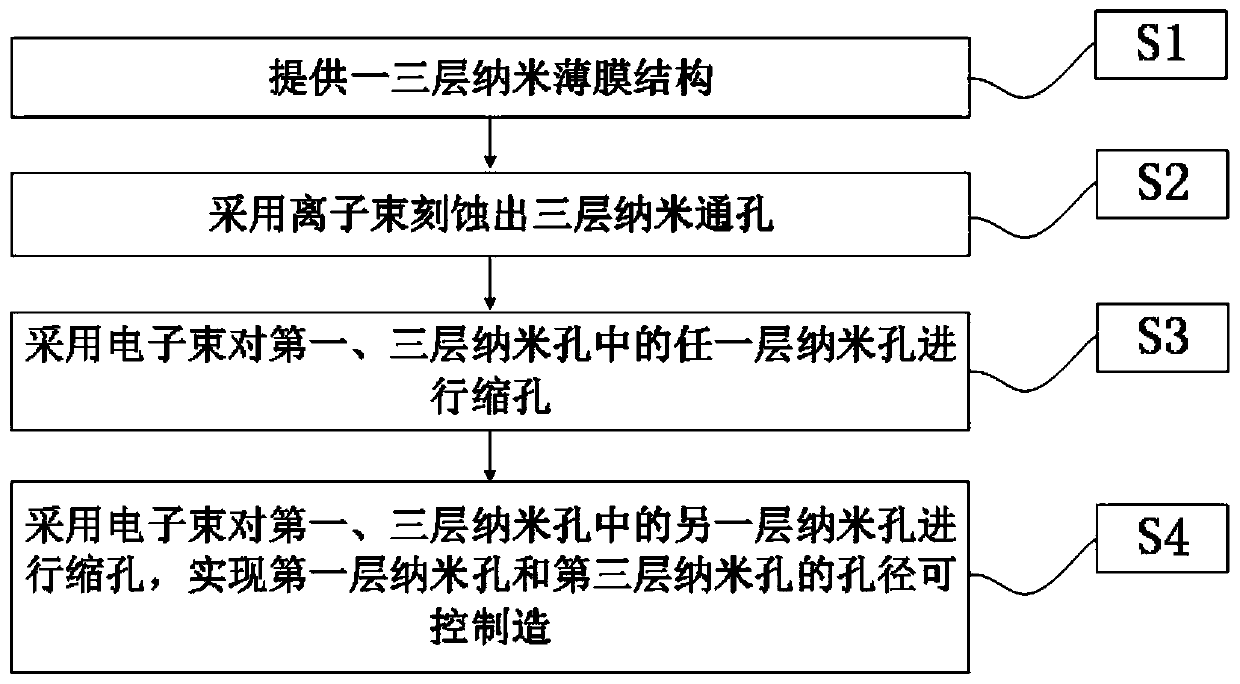
[0056] A size-controllable three-layer nanopore structure and a preparation method thereof, comprising the steps of:
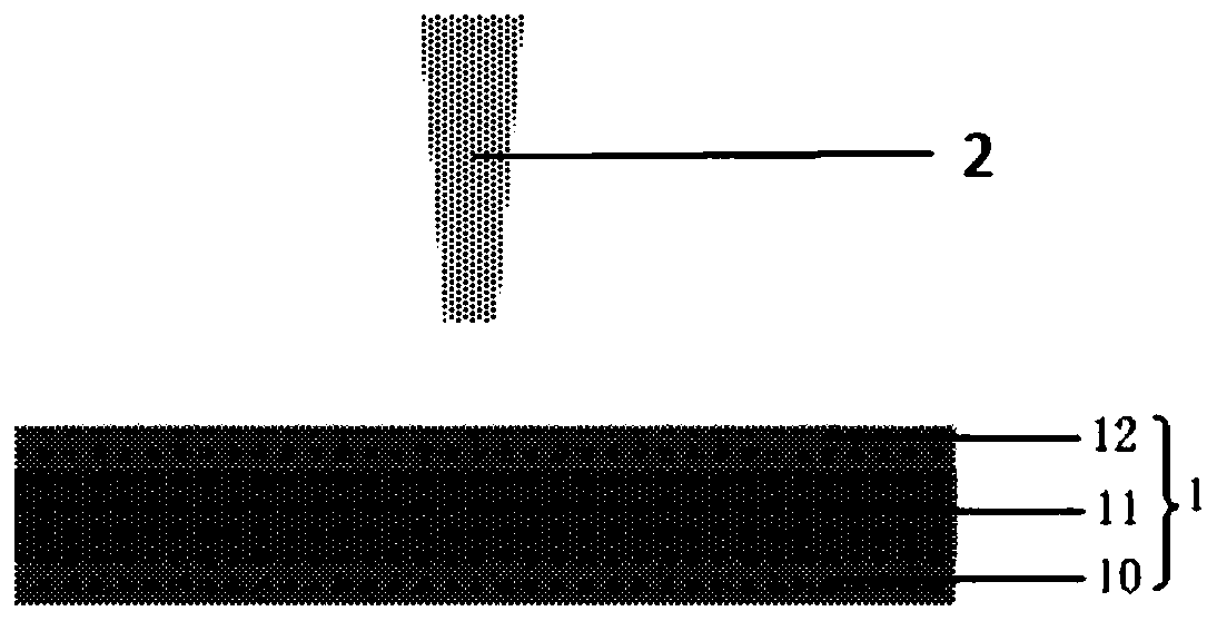
[0057] S1. Provide a three-layer nano-film structure Si 3 N 4 / SiO 2 / Si 3 N 4 ,Such as figure 2 Shown; the first layer of Si 3 N 4 Nanofilm 1 and third layer Si 3 N 4 The thickness of the nano film 2 is 30nm, and the second layer of SiO 2 The thickness of the nano film is 50nm;
[0058] S2. The three-layer nano-film structure is etched by a gallium ion beam to obtain a three-layer nano-through hole with a diameter of 50 nm, such as image 3 and Figure 4 shown;
[0059] S3. Electron beam treatment of the first layer of Si 3 N 4 Nanopore 1 performs shrinkage, such as Figure 6 shown;
[0060] S4. Then use electron beam to treat the third layer of Si 3 N 4 Nanopore 2 is subjected to shrinkage to obtain a three-layer nanopore structure, such as Figure 7 shown;
[0061] In steps S3 and S4, a scanning electron microscope is used to generate ...
Embodiment 2
[0063] A size-controllable three-layer nanopore structure and a preparation method thereof, comprising the steps of:
[0064] S1. Provide a three-layer nano-film structure Si 3 N 4 / Si / Si 3 N 4 ; the first layer of Si 3 N 4 Nanofilm and third layer Si 3 N 4 The thickness of the nano film is 5nm, and the thickness of the second layer of Si nano film is 20nm;
[0065] S2. Etching the three-layer nano-film structure with a helium ion beam to obtain a three-layer nano-through hole with a diameter of 50 nm;
[0066] S3. Using electron beam to treat the third layer of Si 3 N 4 Nanopores for shrinkage;
[0067] S4. Then use electron beam to treat the first layer of Si 3 N 4 The nanopores are shrunk to obtain a three-layer nanopore structure;
[0068] In steps S3 and S4, a scanning electron microscope is used to generate an electron beam. The parameters of the electron beam are as follows: the electron beam voltage is 0.5kV, the electron beam current is 0.5µA, the contin...
Embodiment 3
[0070] A size-controllable three-layer nanopore structure and a preparation method thereof, comprising the steps of:
[0071] S1. Provide a three-layer nano-film structure SiO 2 / Si / SiO 2 ; the first layer of SiO 2 Nanofilm and third layer SiO 2 The thickness of the nano film is 50 nm, and the thickness of the second Si nano film is 200 nm;
[0072] S2. Using gallium ion beams to etch the three-layer nano-film structure to obtain a three-layer nano-through hole with a diameter of 300nm;
[0073] S3. Electron beam treatment of the first layer of SiO 2 Nanopores for shrinkage;
[0074] S4. Then electron beam is used to treat the third layer of SiO 2 The nanopores are shrunk to obtain a three-layer nanopore structure;
[0075] In steps S3 and S4, a transmission electron microscope is used to generate an electron beam. The parameters of the electron beam are as follows: the electron beam voltage is 20kV, the electron beam current is 50µA, the continuous scanning time is 5...
PUM
| Property | Measurement | Unit |
|---|---|---|
| thickness | aaaaa | aaaaa |
| diameter | aaaaa | aaaaa |
| pore size | aaaaa | aaaaa |
Abstract
Description
Claims
Application Information
 - R&D
- Intellectual Property
- Life Sciences
- Materials
- Tech Scout
- Unparalleled Data Quality
- Higher Quality Content
- 60% Fewer Hallucinations
Browse by: Latest US Patents, China's latest patents, Technical Efficacy Thesaurus, Application Domain, Technology Topic, Popular Technical Reports.
© 2025 PatSnap. All rights reserved.Legal|Privacy policy|Modern Slavery Act Transparency Statement|Sitemap|About US| Contact US: help@patsnap.com


