Fabrication method of integrated silicon-based visible light detector array device

A detector array and integrated silicon-based technology, applied in semiconductor devices, electrical components, radiation control devices, etc., can solve the problems that APD cannot meet high blue light sensitivity, wide band full coverage and high cut-off frequency at the same time, and achieve blue light response The effect of improving the degree, improving the quantum efficiency, and reducing the photosensitive area

Active Publication Date: 2022-02-01
CHANGCHUN INST OF OPTICS FINE MECHANICS & PHYSICS CHINESE ACAD OF SCI
View PDF6 Cites 0 Cited by
  • Summary
  • Abstract
  • Description
  • Claims
  • Application Information

AI Technical Summary

Problems solved by technology

[0005] In view of this, the present invention provides a method for manufacturing an integrated silicon-based visible light detector array device in order to solve the technical problems of APDs in the prior art that cannot simultaneously satisfy high blue light sensitivity, wide-band full coverage, and high cut-off frequency

Method used


Image

  • Fabrication method of integrated silicon-based visible light detector array device
  • Fabrication method of integrated silicon-based visible light detector array device
  • Fabrication method of integrated silicon-based visible light detector array device

Examples


specific Embodiment approach 1

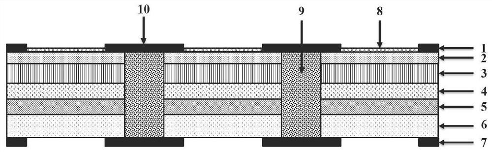
[0058] DETAILED DESCRIPTION OF THE PREFERRED EMBODIMENT 1. This embodiment is described with reference to FIGS. 1 to 5 . The integrated silicon-based visible light detector array device provided by this embodiment includes multiple detection units, multiple isolation regions 9 and multiple electrode leads 10 .

[0059] Among them, a plurality of detection units are regularly arranged to form an array, and each detection unit includes an anode 1, a non-depletion layer 2, an absorption layer 3, a field control layer 4, an avalanche layer 5, a substrate layer 6, a cathode 7 and a light-transmitting layer 8. The field control layer 4 , the absorption layer 3 and the non-depletion layer 2 are sequentially arranged on the upper surface of the avalanche layer 5 from bottom to top. Both the transparent layer 8 and the anode 1 are arranged on the upper surface of the non-depleted layer 2, and the lower surface of the anode 1 is in contact with the upper surface of the non-depleted laye...

specific Embodiment approach 2

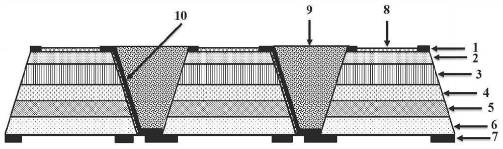
[0066] Specific embodiment 2. For the parallel electrode structure array device, and the light-transmitting layer 8 and the anode 1 are all located on the same plane, combined with Figure 6 To illustrate the present embodiment, the basic process steps are as follows:

[0067] Step 1. Select a highly doped n+ type silicon wafer as the substrate material of the array device, and perform cleaning treatment; the impurities are pentavalent elements such as P and As.

[0068] Step 2. Deposit a silicon epitaxial layer on the substrate material by techniques such as vapor phase epitaxy (VPE) or molecular beam epitaxy (MBE), as the avalanche layer 5 of the array device; the grown epitaxial material is silicon with low doping concentration and low defect .

[0069] Step 3: growing a p-type Si field control layer 4 on the avalanche layer 5 by vapor phase epitaxy or molecular beam epitaxy.

[0070] Step 4: After the field control layer 4 is prepared, a p-type Si-based absorption layer ...

specific Embodiment approach 3

[0087] Specific embodiment 3. The manufacturing process for the case where a part of the lower surface of the light-transmitting layer 8 of the array device is in contact with the non-depleted layer 2, and the remaining part is in contact with the upper surface of the anode 1: step 10 in the specific embodiment 2 Step 3 and step 14 are combined and changed to: prepare an anti-reflection film with a thickness of about 0.1-5 μm on the upper surface of the non-depleted layer 2 and the anode 1 by low-temperature evaporation method as the light-transmitting layer 8 of the array device.


PUM

PropertyMeasurementUnit
thicknessaaaaaaaaaa
thicknessaaaaaaaaaa
thicknessaaaaaaaaaa

Abstract

The invention discloses a manufacturing method of an integrated silicon-based visible light detector array device, belonging to the field of optoelectronic technology. It provides a high integration of silicon-based visible light avalanche photodiode array and a manufacturing process method of complex connection modes between highly integrated detection units. In the manufacturing method of the present invention, an epitaxial layer is first deposited on the cleaned substrate material as an avalanche layer, then a field control layer is deposited on the avalanche layer, then an absorption layer is deposited on the field control layer, and then an absorption layer is deposited on the absorption layer Deposit the non-depletion layer, then prepare the isolation area, then prepare the anode and the anode electrode lead, then prepare the light-transmitting layer, then thin the substrate until the isolation area is exposed, form the substrate layer, and finally prepare the cathode and the cathode electrode lead, remove The substrate is used to obtain an integrated silicon-based visible light detector array device. The array device manufactured by the manufacturing method has high blue light responsivity and high quantum efficiency in the full band of visible light.

Description

technical field [0001] The invention belongs to the field of optoelectronic technology, and in particular relates to a manufacturing method of an integrated silicon-based visible light detector array device. Background technique [0002] An avalanche photodiode (APD) is a photosensitive element commonly used in the field of optical communications. After a reverse bias is applied to the P-N junction of a photodiode made of silicon or germanium, the incident light will be absorbed by the P-N junction to form a photocurrent, and increasing the reverse bias will produce an "avalanche" ( That is, the photocurrent exponentially increases), this kind of diode is called "avalanche photodiode". [0003] The working principle of the avalanche photodiode is to use the directional movement of photo-generated carriers in a strong electric field to generate an avalanche effect to obtain the gain of photocurrent. In the avalanche process, the photogenerated carriers move in a high-speed ...

Claims


Application Information

Patent Timeline
Patent Type & Authority Patents(China)
IPC IPC(8): H01L31/18H01L27/144H01L31/0216H01L31/0224H01L31/0232H01L31/0352H01L31/107
Inventor 梁静秋秦余欣张军高丹王维彪吕金光陶金陈锋
Owner CHANGCHUN INST OF OPTICS FINE MECHANICS & PHYSICS CHINESE ACAD OF SCI
Why Eureka
Try Eureka