
Preparation method of solar cell

A solar cell and silicon wafer technology, applied in circuits, photovoltaic power generation, electrical components, etc., can solve the problems of abnormal square resistance, difficult operation, inconvenient operation, etc., and achieve the effect of easy removal, low process difficulty, and wide operation window.

Inactive Publication Date: 2019-04-26
ZHEJIANG JINKO SOLAR CO LTD +1
View PDF9 Cites 4 Cited by
  • Summary
  • Abstract
  • Description
  • Claims
  • Application Information

AI Technical Summary

Problems solved by technology

[0007] In the method of preparing a silicon nitride mask layer with a reasonable refractive index using a mask matching the emitter screen, the refractive index and film thickness are difficult to accurately control, and the HF etching of silicon nitride takes a long time and is inconvenient to operate; When the non-electrode area is corroded by weak alkali and hydrogen peroxide, the solution will corrode the metal electrode area, resulting in abnormal square resistance, and the operation is difficult

Method used


Image

  • Preparation method of solar cell
  • Preparation method of solar cell

Examples


Embodiment Construction

[0031] The following will clearly and completely describe the technical solutions in the embodiments of the present invention with reference to the accompanying drawings in the embodiments of the present invention. Obviously, the described embodiments are only some, not all, embodiments of the present invention. Based on the embodiments of the present invention, all other embodiments obtained by persons of ordinary skill in the art without making creative efforts belong to the protection scope of the present invention.

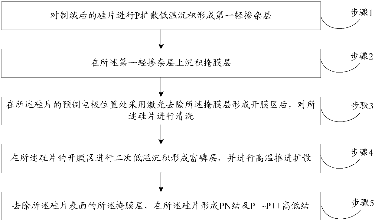
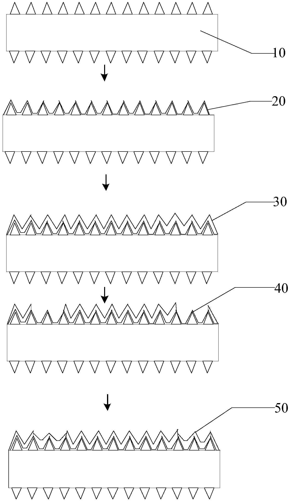
[0032] Please refer to figure 1 , figure 1 A schematic flow chart of the steps of a specific implementation of the solar cell preparation method provided by the embodiment of the present invention; figure 2 It is a schematic process flow diagram of a specific implementation mode of the solar cell manufacturing method provided in the embodiment of the present invention.

[0033] In a specific embodiment, the solar cell preparation method includes:

[0034] ...


PUM


Abstract

The invention discloses a preparation method of a solar cell. The preparation method comprises the following steps: 1, conducting P diffusion low-temperature deposition on a textured silicon wafer toform a first lightly doped layer; 2, depositing a mask layer on the first lightly doped layer; 3, after the mask layer is removed by laser at the position of a prefabricated electrode of the silicon wafer to form a film opening area, and cleaning the silicon wafer; 4, conducting secondary low-temperature deposition on the film opening area of the silicon wafer to form a phosphorus-rich layer; 5, removing the mask layer on the surface of the silicon wafer, and forming PN junctions and P +-P ++ high-low junctions on the silicon wafer. The lightly doped layer is firstly formed on the surface of the textured silicon wafer, then a mask layer is arranged, the first lightly doped layer at the electrode area is removed by laser to form the film opening area, then the phosphorus-rich layer is deposited in the film opening area, and the PN junctions and the P +-P ++ high-low junctions are prepared in a one-step knot pushing mode. Since light expansion and the square resistance of a re-diffusionarea can be optionally adjusted, an operation window is wide, additionally the mask layer is easily removed, and the process difficulty is low.

Description

technical field [0001] The invention relates to the technical field of solar cell preparation, in particular to a solar cell preparation method. Background technique [0002] Since the use of solar cells for power generation has lower requirements on the site and less pollution, it is a new type of energy. Due to the continuous development of its technology, the cost of power generation has been greatly reduced, and thus it has been widely used. [0003] Efficient and highly reliable solar cells are one of the factors that reduce the cost of power generation. [0004] Conventional solar cells use diffusion to prepare uniform junctions. The high doping concentration of the diffusion layer leads to high Auger recombination, which reduces the minority carrier lifetime, and a high-quality passivation film is required to passivate the doped layer with high surface concentration in the subsequent passivation process. The emergence of the selective emitter, on the one hand, ensure...

Claims


Application Information

Patent Timeline
Patent Type & Authority Applications(China)
IPC IPC(8): H01L21/225H01L31/18
CPCH01L21/2252H01L31/1804Y02E10/547Y02P70/50
Inventor 廖晖包健徐冠群李明左严严白明华金浩张昕宇
Owner ZHEJIANG JINKO SOLAR CO LTD
Learn More