Multi-chip stacked packaging method and multi-chip stacked package body

A technology of stacking packages and packaging methods, which is applied in the manufacture of semiconductor devices, electrical solid devices, semiconductor/solid devices, etc., can solve problems such as increased impedance, poor heat dissipation mechanism, poor heat conduction, etc., and achieves improved thermal conductivity and packaging Thin thickness, good electrical conductivity

Pending Publication Date: 2019-04-19
HEFEI SMAT TECH CO LTD
View PDF0 Cites 0 Cited by
  • Summary
  • Abstract
  • Description
  • Claims
  • Application Information

AI Technical Summary

Problems solved by technology

Generally speaking, the BGA structure can provide high-density interconnection configuration in the surface area of ​​the package, but the typical BGA package has a circuitous signal path, which will increase the impedance and cause heat dissipation due to poor heat conduction. Mechanism variation

Method used


Image

  • Multi-chip stacked packaging method and multi-chip stacked package body
  • Multi-chip stacked packaging method and multi-chip stacked package body
  • Multi-chip stacked packaging method and multi-chip stacked package body

Examples


Embodiment Construction

[0020] The specific implementation manners of the multi-chip stack packaging method and the multi-chip stack package body provided by the present invention will be described in detail below with reference to the accompanying drawings.

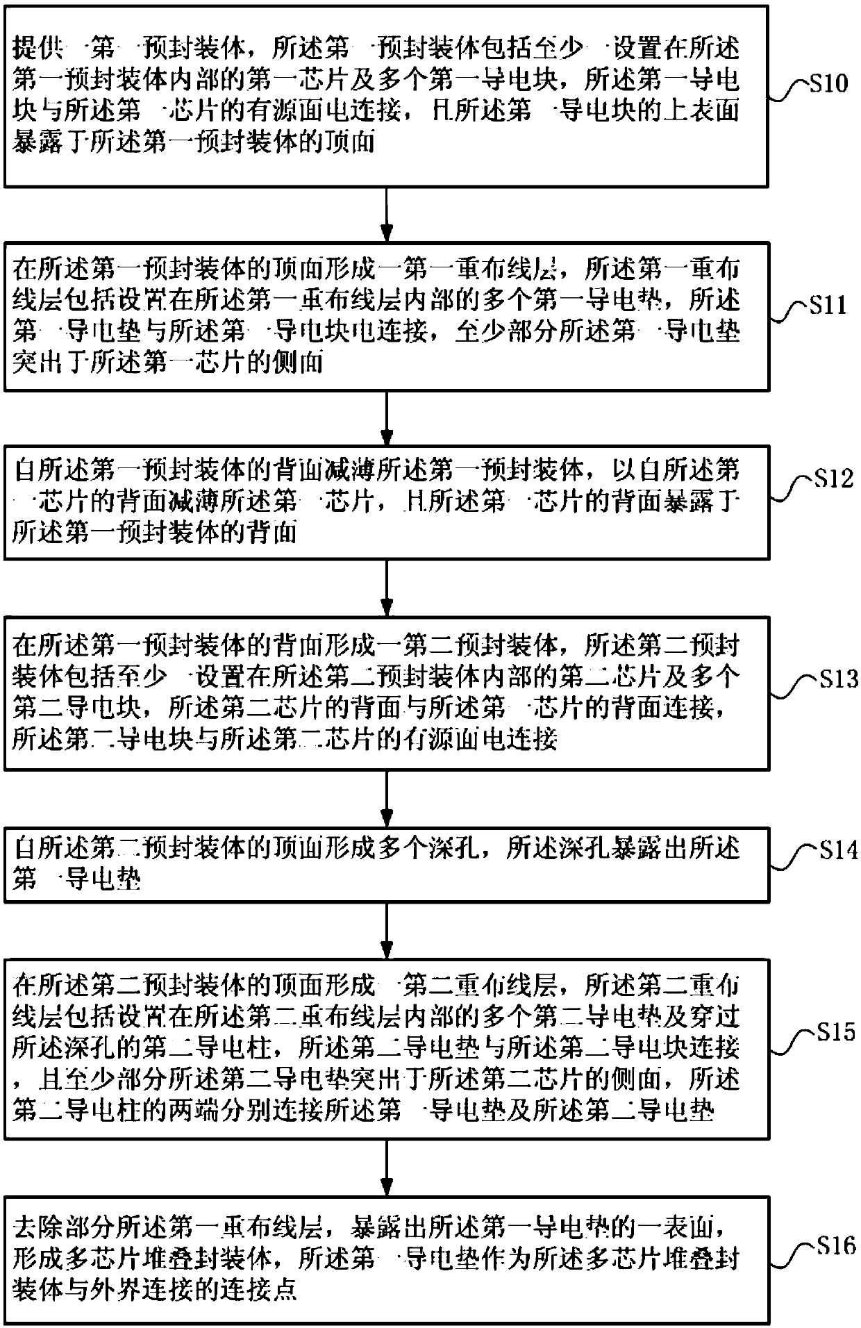
[0021] figure 1 It is a schematic diagram of the steps of the multi-chip stack packaging method of the present invention. see figure 1The multi-chip stack packaging method of the present invention includes the following steps: step S10, providing a first pre-package body, the first pre-package body including at least one first chip disposed inside the first pre-package body and a plurality of A first conductive block, the first conductive block is electrically connected to the active surface of the first chip, and the upper surface of the first conductive block is exposed to the top surface of the first prepackage body; step S11, A first redistribution layer is formed on the top surface of the first prepackage, the first redistribution layer ...


PUM


Abstract

The invention provides a multi-chip stacked packaging method and a multi-chip stacked package body. The method has the advantages that the interconnection between the stacked chips is realized by useof the combination of the redistribution layer and the conductive pillars; the method replaces the commonly used routing technique and substrate inversion technique for traditional package of stackedchips; and compared with the traditional chip-stacked layer BGA package, the overall package thickness is quite small, the package size is quite small under the condition of the same number of chips,and good electrical conductivity, thermal conductivity and reliability are achieved.

Description

technical field [0001] The invention relates to the field of semiconductor packaging, in particular to a multi-chip stack packaging method and a multi-chip stack package body. Background technique [0002] In recent years, the packaging technology of integrated circuits (chips) has gradually become a bottleneck in the development of high-performance integrated circuits. Miniaturization and multi-chip module (multi-chips module, MCM) packaging structures have been widely used in electronic devices. The multi-chip module package mainly includes two or more dies coated in it to improve the electrical properties and performance of the package. [0003] Today's packaging technology gradually tends to adopt ball grid array package (ball grid array, BGA), flip chip ball grid array package (flip chip ball grid array, FC-BGA), chip size package (chip size package, CSP), wafer Level packaging (Wafer Level Package, WLP) technology. Generally speaking, the BGA structure can provide hi...

Claims


Application Information

Patent Timeline
IPC IPC(8): H01L21/98H01L25/18H01L23/367H01L23/31
CPCH01L25/18H01L25/50H01L23/3107H01L23/367H01L2224/18H01L2224/2413
Inventor 张光耀陆培良
Owner HEFEI SMAT TECH CO LTD
Why Eureka
Try Eureka