
A highly balanced reverse on-chip capacitor pair structure

A balanced and reverse technology, applied in the direction of capacitors, circuits, electrical components, etc., to achieve the effect of improving symmetry, high Q value characteristics, and realizing impedance matching

Pending Publication Date: 2019-03-26
SOUTHEAST UNIV
View PDF3 Cites 1 Cited by
  • Summary
  • Abstract
  • Description
  • Claims
  • Application Information

AI Technical Summary

Problems solved by technology

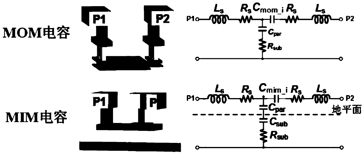
But as the frequency increases, 1 / jωC par The value decreases, and because the resistivity of the silicon-based semiconductor process substrate is lower, so R sub The value of is also small, so that D eff It is positively correlated with frequency, resulting in different capacitance values ​​for single MOM and MIM capacitors from the two ports.

Method used


Image

  • A highly balanced reverse on-chip capacitor pair structure
  • A highly balanced reverse on-chip capacitor pair structure
  • A highly balanced reverse on-chip capacitor pair structure

Examples


Embodiment Construction

[0035] The technical solution of the present invention will be further introduced below in combination with specific implementation methods and accompanying drawings.

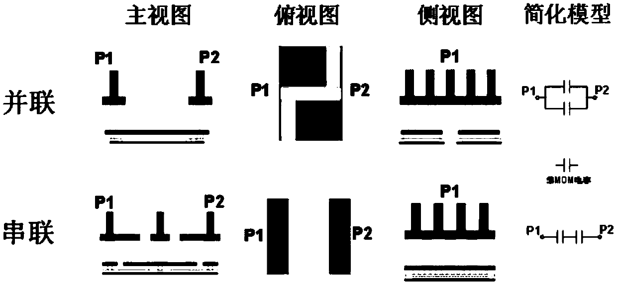
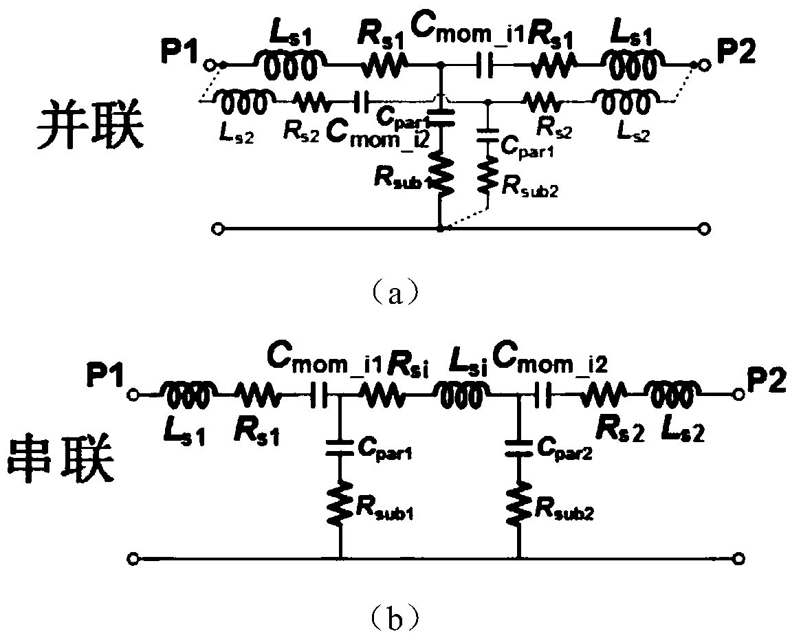
[0036] This specific embodiment discloses a highly balanced reverse on-chip capacitor pair structure, which includes a pair of reversely placed capacitor units. The capacitor unit is a metal-oxide-metal structure, which is formed by stacking metal layers and silicon dioxide layers. Capacitor cells can be connected in series, such as figure 2 and image 3 (a) shown. Capacitor units can also be connected in parallel, such as figure 2 and image 3 (b) shown. The capacitance value obtained by parallel connection is twice that of the capacitor unit, and the capacitance value obtained by series connection is one-half of the capacitor unit. The reverse capacitor pair structure can eliminate the asymmetry caused by the parasitic effect of the substrate in the millimeter wave and higher frequency bands of the tr...


PUM


Abstract

The invention discloses a reverse on-chip capacitor pair structure with high balance, which comprises a pair of capacitor units arranged in reverse direction. Because capacitors are widely used in matching networks in millimeter-wave circuits, the asymmetry of capacitors affects the characteristics of matching networks. On-chip transformers, as common devices in differential circuits, are sensitive to the asymmetry of capacitors. The invention solves the asymmetry caused by the parasitic effect of the substrate and the like under the millimeter wave and higher frequency bands of the traditional single MOM capacitor, greatly improves the symmetry of the capacitor as a two-port passive device, and improves the balance of the passive network including the on-chip transformer. The invention has two connection modes of parallel connection and series connection, and has higher expansibility. The invention can be combined with on-chip transformer and other components to optimize, improve thebalance of the differential circuit, achieve impedance matching and other functions, thereby improving the millimeter wave and higher frequency circuit performance, including the output power and energy conversion efficiency of the power amplifier.

Description

technical field [0001] The invention relates to the field of semiconductor integrated circuits, in particular to a highly balanced reverse on-chip capacitance pair structure. Background technique [0002] With the rapid development of silicon-based semiconductor technology, its cut-off frequency and the highest power transmission frequency have exceeded 500GHz, comparable to III-V semiconductor technology. In addition, due to the low cost, high flexibility, and integration of digital and analog features of the silicon-based process, the silicon-based millimeter-wave system has become a research hotspot in academia and industry, including the 5G millimeter-wave broadband ultra-high-speed communication system (WRC-19 1.13), W-band long-distance millimeter-wave automotive radar, terahertz imaging technology, etc. However, due to the low substrate resistivity of the silicon-based process and the small spacing between metal layers, there are many parasitic effects. The parasiti...

Claims


Application Information

Patent Timeline
Patent Type & Authority Applications(China)
IPC IPC(8): G06F17/50H01L23/64
CPCH01L23/642H01L28/40G06F30/392G06F2115/06G06F30/20
Inventor 侯德彬李焕波严蘋蘋陈继新洪伟
Owner SOUTHEAST UNIV
Learn More