


Quick Research
Generate reliable direction feasibility study reports for your R&D in just a few steps.

Technical Q&A
Discover and master advanced knowledge NOW. Basics, ideas, possibilities, all at once.

Find Solutions
As an expert in R&D theories, this can generate solutions to your technical problems instantly.

Evaluate Feasibility
Analyze your overall solution with one click, know your potential R&D risks in advance.

Monitor Landscape
Get weekly tech updates, stay abreast of the latest tech innovations and key insights.
Organic electroluminescent device and preparation method and display device thereof
An electroluminescent device and luminescent technology, which is applied in the fields of electric solid-state devices, semiconductor/solid-state device manufacturing, electrical components, etc., can solve problems such as high triplet exciton concentration, device stability decline, triplet exciton annihilation, etc. , to achieve the effect of inhibiting molecular bond breakage, improving stability and reducing long life
- Summary
- Abstract
- Description
- Claims
- Application Information
AI Technical Summary
Problems solved by technology
Method used
Image

Examples
preparation example Construction
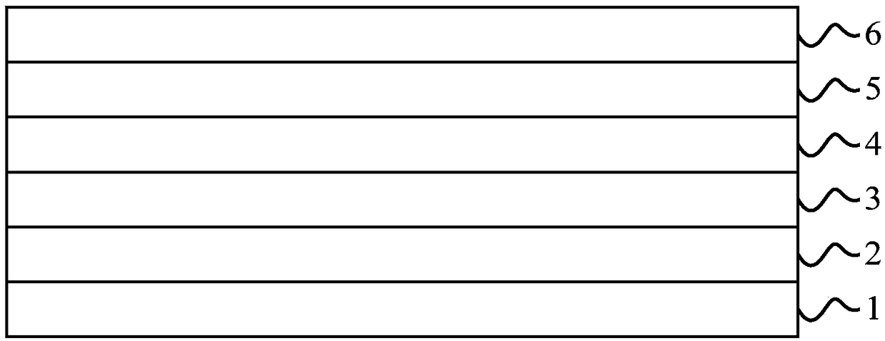
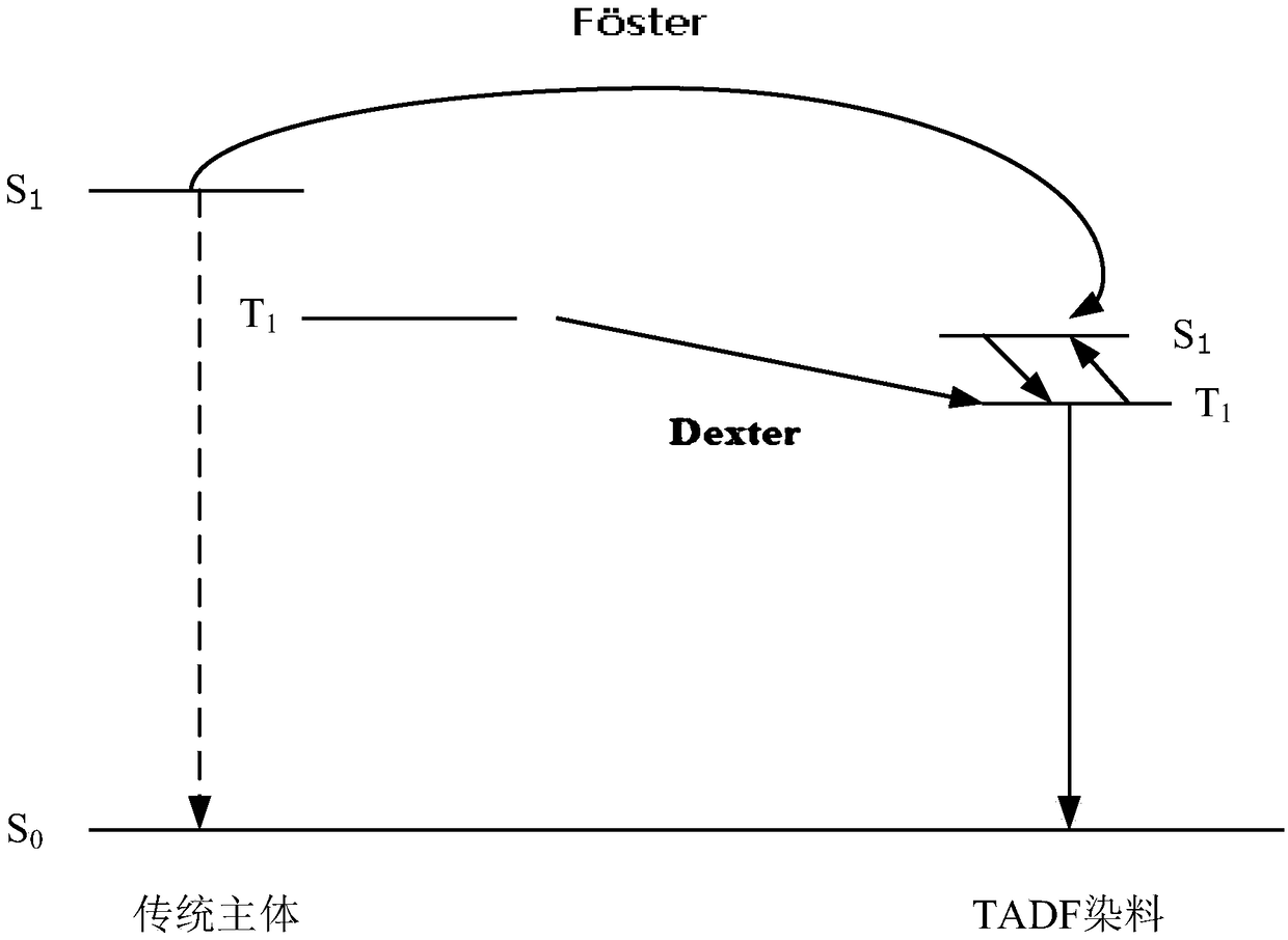
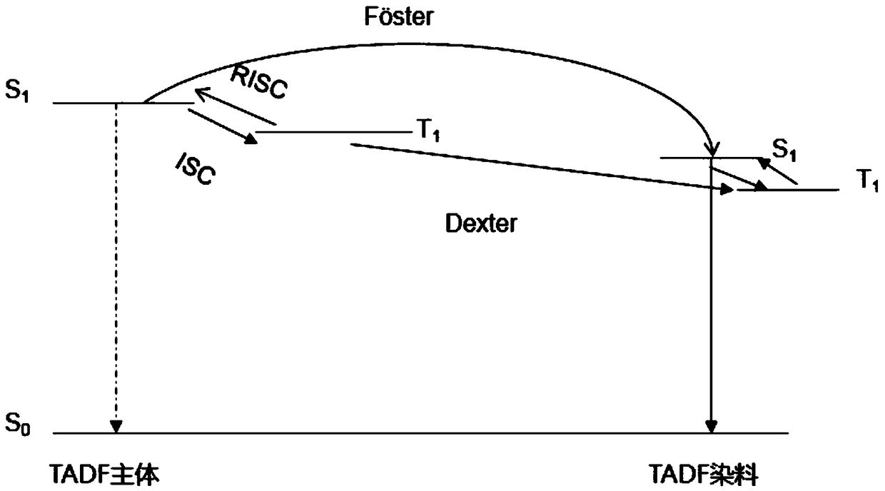
[0072] The present invention also provides a preparation method of the organic electroluminescent device, to figure 1 As an example, it includes sequentially depositing an anode 2 , a hole transport region 3 , a light emitting layer 4 , an electron transport region 5 , and a cathode 6 on a substrate 1 , and then packaging. Wherein, when preparing the light emitting layer 4, the light emitting layer 4 is formed by co-evaporating the triplet-triplet annihilation material source and the thermally activated delayed fluorescent material source.
[0073] Specifically, the preparation method of the organic electroluminescent device of the present invention comprises the following steps:
[0074] 1. Ultrasonically treat the glass plate coated with the anode material in a commercial cleaning agent, rinse in deionized water, ultrasonically degrease in acetone: ethanol mixed solvent, bake in a clean environment until the water is completely removed, and use ultraviolet light Light and o...
Embodiment 1-21
[0083] Embodiment 1-21 provides a kind of organic electroluminescent device respectively, and its device structure comprises ITO anode, hole injection layer (HIL), hole transport layer (HTL), light-emitting layer (EML), electron transport layer (ETL) successively. ), the electron injection layer (EIL) and the cathode.
[0084] Wherein, the material of the hole injection layer is HI-2, and the general total thickness is 5-30nm, which is 10nm in this embodiment. The material of the hole transport layer is HT-28, and the total thickness is generally 5-50 nm, which is 50 nm in this embodiment. The host material of the light-emitting layer is TTA material, the dye is TADF material, the doping concentration of the dye is 0.1-40wt%, and the thickness of the light-emitting layer is generally 1-60nm, which is 30nm in this embodiment. The material of the electron transport layer is ET-53, and the thickness is generally 5-30nm, which is 30nm in this embodiment. LiF (0.5nm) and metal al...
PUM
| Property | Measurement | Unit |
|---|---|---|
| Thickness | aaaaa | aaaaa |
| Thickness | aaaaa | aaaaa |
Abstract
Description
Claims
Application Information
 - R&D Engineer
- R&D Manager
- IP Professional
- Industry Leading Data Capabilities
- Powerful AI technology
- Patent DNA Extraction
Browse by: Latest US Patents, China's latest patents, Technical Efficacy Thesaurus, Application Domain, Technology Topic, Popular Technical Reports.
© 2024 PatSnap. All rights reserved.Legal|Privacy policy|Modern Slavery Act Transparency Statement|Sitemap|About US| Contact US: help@patsnap.com