Large-area efficient stable passivated tunneled organic-inorganic hybrid perovskite solar cell and laminated cell
A solar cell and perovskite technology, applied in the field of solar cells, can solve problems such as leakage, low battery efficiency, and low photoelectric conversion efficiency of crystalline silicon stacked cells, so as to solve battery leakage, improve electrical contact, and avoid severe battery efficiency. Falling effect
- Summary
- Abstract
- Description
- Claims
- Application Information
AI Technical Summary
Problems solved by technology
Method used
Image
Examples
Embodiment 1
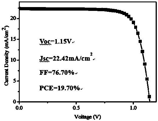
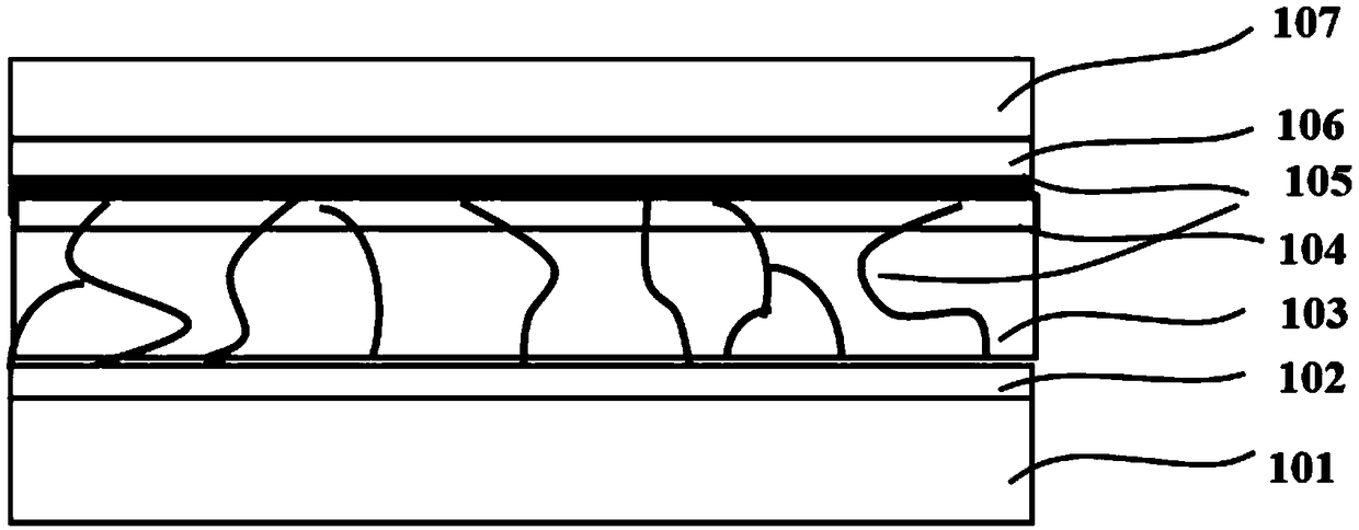
[0038] Schematic diagram of the structure of a large-area high-efficiency organic-inorganic hybrid perovskite solar cell (A). figure 1 As shown, it includes a conductive glass substrate 101, an electron transport layer 102, a perovskite light absorption layer 103, a hole transport layer 104, an ALD passivation layer 105, a heavily doped hole transport layer 106 and a metal electrode 107, that is, from a conductive glass The substrate 101 is sequentially provided with an electron transport layer 102 , a perovskite light absorbing layer 103 , a hole transport layer 104 , an ALD passivation layer 105 , a heavily doped hole transport layer 106 and a metal electrode 107 from bottom to top. Wherein, the conductive glass substrate 101 is FTO conductive glass, and the electron transport layer 102 can be TiO 2 or SnO 2 , the material of the perovskite light absorbing layer 103 can be MAPbI 3 , CsxMA1-xPbI 3 (x=0~0.3)MAPbI 3 -xBrx (x=0~0.2), FAPbI 3 etc., the hole transport layer 1...
Embodiment 2
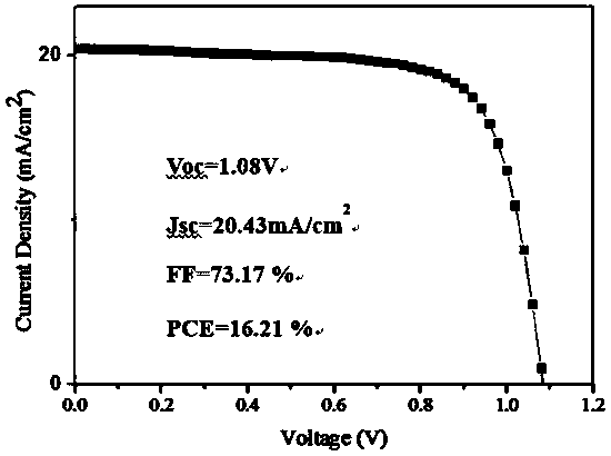
[0052] Schematic diagram of the structure of a large-area high-efficiency organic-inorganic hybrid perovskite solar cell (B). Figure 4 As shown, it includes a conductive glass substrate 101, a hole transport layer 104, a perovskite light absorption layer 103, an electron transport layer 102, an ALD passivation layer 105, a heavily doped electron transport layer 108 and a metal electrode 107, that is, from a conductive glass substrate 101 is sequentially arranged from bottom to top as a hole transport layer 104 , a perovskite light absorption layer 103 , an electron transport layer 102 , an ALD passivation layer 105 , a heavily doped electron transport layer 108 and a metal electrode 107 . Wherein, the conductive glass substrate 101 is FTO conductive glass, the hole transport layer 104 can be NiO etc., the material of the perovskite light absorbing layer 103 can be MAPbI 3 , Cs x MA 1-x PB 3 (x=0~0.3)MAPbI 3-x Br x (x=0~0.2), FAPbI 3 etc., the electron transport layer 10...
Embodiment 3
[0064] Schematic diagram of the large-area high-efficiency organic-inorganic hybrid perovskite / HIT crystalline silicon tandem solar cell (C). Figure 5 As shown, it includes a metal electrode 116, a transparent conductive layer 115, an n-type a-Si:H layer 114, an intrinsic a-Si:H layer 113, an n-type single crystal silicon substrate 112, and an intrinsic a-Si:H layer 111. p-type a-Si: H layer 110, transparent conductive layer 117, electron transport layer 102, organic-inorganic hybrid perovskite light absorption layer 103, hole transport layer 104, nitride deposited by ALD 105, heavy doping A hole transport layer 106 , a transparent conductive layer 118 , and a metal grid line 109 . Among them, 116 is an Al or Ag electrode, 115 is ITO, 114 is a-Si:H doped with phosphorus, 110 is a-Si:H doped with boron, the transparent conductive layer 117 is ITO, and the electron transport layer 102 is TiO 2 or SnO 2 , 103 is MAPbI 3 、Cs x MA 1- x PB 3 (x=0~0.3)MAPbI 3-x Br x (x=0~0....
PUM
 Abstract
Description
Claims
Application Information
 - R&D
- Intellectual Property
- Life Sciences
- Materials
- Tech Scout
- Unparalleled Data Quality
- Higher Quality Content
- 60% Fewer Hallucinations
Browse by: Latest US Patents, China's latest patents, Technical Efficacy Thesaurus, Application Domain, Technology Topic, Popular Technical Reports.
© 2025 PatSnap. All rights reserved.Legal|Privacy policy|Modern Slavery Act Transparency Statement|Sitemap|About US| Contact US: help@patsnap.com


