Semiconductor structure and formation method thereof

A semiconductor and layer-forming technology, used in semiconductor devices, semiconductor/solid-state device manufacturing, electrical components, etc., can solve problems such as poor electrical performance of transistors and poor semiconductor structure performance, and achieve improved threshold voltage inversion, lower threshold voltage, and increased The effect of aluminum atom content

Active Publication Date: 2019-01-29
SEMICON MFG INT (SHANGHAI) CORP +1
View PDF5 Cites 0 Cited by
  • Summary
  • Abstract
  • Description
  • Claims
  • Application Information

AI Technical Summary

Problems solved by technology

[0005] In the prior art, the adjustment of the threshold voltage of the transistor is realized by forming a work function layer in the gate structure of the transistor, but the transistor with the work function layer still has the problem of poor electrical performance, resulting in poor performance of the formed semiconductor structure

Method used


Image

  • Semiconductor structure and formation method thereof
  • Semiconductor structure and formation method thereof
  • Semiconductor structure and formation method thereof

Examples


Embodiment Construction

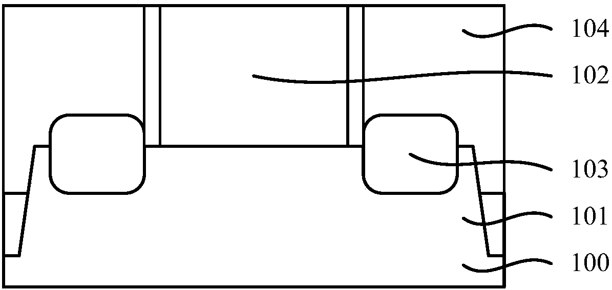
[0030] It can be seen from the background art that the transistors introduced with the work function layer have the problem of poor electrical performance. Combining with a structural schematic diagram of a transistor with a work function layer, the reasons for its poor electrical performance are analyzed:

[0031] refer to figure 1 , shows a schematic structural diagram of a transistor with a work function layer.

[0032] The transistor includes: a substrate 10; an interlayer dielectric layer 11 located on the substrate 10, the interlayer dielectric layer 11 has an opening (not marked) exposing the substrate 10; a gate located in the opening structure, the gate structure includes a gate dielectric layer 12 located at the bottom and sidewalls of the opening, a work function layer 13 located on the gate dielectric layer 12, and a work function layer 13 located on the work function layer 13 and filling the opening The metal layer 14.

[0033] The work function layer 13 is a w...


PUM


Abstract

The invention relates to a semiconductor structure and a formation method thereof. The formation method comprises the steps of providing a substrate; forming an interlayer dielectric layer on the substrate; forming an opening exposing the substrate in the interlayer dielectric layer; forming a gate dielectric layer at the bottom and side wall of the opening; performing a film forming process for at least one time through an atomic layer deposition process, and forming an aluminum-containing work function layer on the gate dielectric layer, wherein the pulse number of an aluminum-containing precursor in the film forming process is at least 2 when the number of times of the film forming process is 1, and the pulse number of the aluminum-containing precursor in the at least one time of the film forming process is at least 2 when the number of times of the film forming process is greater than 1; and forming a metal gate in the opening in which the work function layer is formed. The contentof aluminum atoms in the opening is increased through increasing the pulse number of the aluminum-containing precursor, especially the pulse number in the first time of the film forming process, andthe deposition ability of the aluminum atoms in the opening is improved, thereby increasing the aluminum atom content of the work function layer, and thus improving a problem of threshold voltage flipof transistors.

Description

technical field [0001] The invention relates to the field of semiconductor manufacturing, in particular to a semiconductor structure and a forming method thereof. Background technique [0002] The main semiconductor device of an integrated circuit, especially a very large scale integrated circuit, is a metal-oxide-semiconductor field effect transistor (MOS transistor). With the continuous development of integrated circuit manufacturing technology, the technology nodes of semiconductor devices continue to decrease, and the geometric dimensions of semiconductor devices follow Moore's law. When the size of semiconductor devices is reduced to a certain extent, various secondary effects caused by the physical limits of semiconductor devices appear one after another, and it becomes more and more difficult to scale down the feature size of semiconductor devices. Among them, in the field of semiconductor manufacturing, the most challenging thing is how to solve the problem of large...

Claims


Application Information

Patent Timeline
IPC IPC(8): H01L29/49H01L29/78H01L21/336
CPCH01L29/4958H01L29/66477H01L29/78
Inventor 邓浩徐建华
Owner SEMICON MFG INT (SHANGHAI) CORP
Why Eureka
Try Eureka