A Method for Making Ultra-narrow Line Width and Line Distance Pattern of Metallized Ceramic Substrate
A technology of metallized ceramics and ultra-narrow line width, which is applied in the fields of removing conductive materials by chemical/electrolytic methods, removing conductive materials by mechanical methods, and manufacturing printed circuits. and other problems to achieve the effect of fast processing speed, high efficiency and saving equipment investment
- Summary
- Abstract
- Description
- Claims
- Application Information
AI Technical Summary
Problems solved by technology
Method used
Image

Examples
Embodiment 1
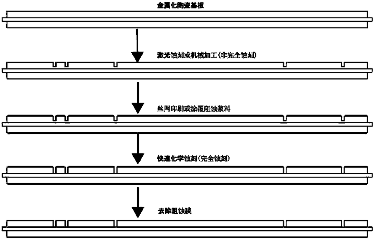
[0041] like figure 1As shown, this case is used for the AlN-DBC ultra-narrow line spacing method, including the following steps: (process flow is as follows figure 1 shown)
[0042] S1. Process the designed graphics on the AlN-DBC copper surface by laser etching to realize the incomplete Etching, graphic line width and line spacing are 100μm, laser etching depth is 250μm±30μm.
[0043] S2. Print the organic anti-corrosion paste on the upper part of the etched figure by a screen printing machine, and the thickness of the printing paste is about 20 μm. The organic corrosion resist paste in this embodiment is green solder resist ink.
[0044] S3, curing the anti-corrosion slurry covering the graphic surface by drying.
[0045] S4, and then chemical etching is used to etch away the remaining metal copper at the bottom of the wire groove to achieve complete etching, and the chemical etching solution is hydrochloric acid and sodium chlorate.
[0046] S5, passing the chemically ...
Embodiment 2
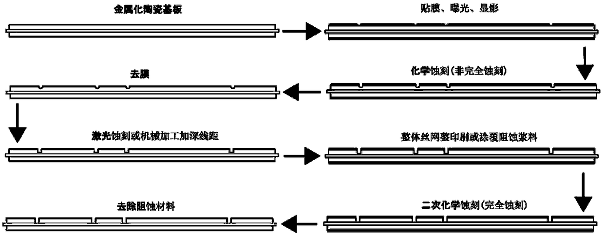
[0048] This case is used for Al 2 o 3 -DBC ultra-narrow line width and line spacing method, comprising the following steps:
[0049] S1. Al with specifications of 127mm*127mm*1.00mm (copper specification 124mm*124mm*0.60mm) 2 o 3 -DBC ceramic substrate, the designed graphics are placed on Al by mechanical processing 2 o 3 - The copper side of the DBC is machined out for incomplete etching. The graphic line width and line spacing are 300μm, and the machining depth is 550μm±30μm.
[0050] S2. Printing the organic anti-corrosion paste on the upper part of the etched figure by a screen printing machine. The printing paste thickness is about 20 μm. Here, the organic anti-corrosion slurry is a revision ink.
[0051] S3, curing the anti-corrosion slurry covering the graphic surface by drying.
[0052] S4, and then remove the metal copper remaining at the bottom of the line groove by chemical etching to achieve complete etching, and the chemical etching solution is hydrochlor...
Embodiment 3
[0055] This case is used for Si3N4-AMB ultra-narrow line width and line spacing method, including the following steps:
[0056] S1. Machining the Si3N4-AMB ceramic substrate with specifications of 127mm*127mm*0.32mm (copper specification 124mm*124mm*0.40mm) on the copper surface of Si3N4-AMB by mechanical processing to realize incomplete etch. The graphic line width and line spacing are 200μm, and the machining depth is 350μm±30μm.
[0057] S2. Printing the organic anti-corrosion paste on the upper part of the etched figure by a screen printing machine. The printing paste thickness is about 20 μm. Here the organic corrosion resist paste is solder resist ink.
[0058] S3, curing the anti-corrosion slurry covering the graphic surface by drying.
[0059] S4, and then remove the residual metal copper at the bottom of the wire groove by chemical time to achieve complete etching.
[0060] S5 , removing the corrosion-resistant slurry from the chemically etched ceramic substrate ...
PUM
| Property | Measurement | Unit |
|---|---|---|
| thickness | aaaaa | aaaaa |
| thickness | aaaaa | aaaaa |
Abstract
Description
Claims
Application Information
 - R&D
- Intellectual Property
- Life Sciences
- Materials
- Tech Scout
- Unparalleled Data Quality
- Higher Quality Content
- 60% Fewer Hallucinations
Browse by: Latest US Patents, China's latest patents, Technical Efficacy Thesaurus, Application Domain, Technology Topic, Popular Technical Reports.
© 2025 PatSnap. All rights reserved.Legal|Privacy policy|Modern Slavery Act Transparency Statement|Sitemap|About US| Contact US: help@patsnap.com