Silicon carbide material-based Schottky micro nuclear battery and preparation method thereof

A technology of silicon carbide and nuclear batteries, which is applied in the field of Schottky micro-nuclear batteries and its preparation, can solve the problems of limited surface area of ​​the transducing unit, lower energy conversion efficiency, and low doping concentration of the P-type layer, so as to improve the current output performance, improve energy conversion efficiency, and facilitate fast collection effects

Active Publication Date: 2019-01-11
SHANXI DATONG UNIV
View PDF8 Cites 2 Cited by
  • Summary
  • Abstract
  • Description
  • Claims
  • Application Information

AI Technical Summary

Problems solved by technology

[0004] Although there have been researches on silicon carbide nuclear batteries at home and abroad, the conversion efficiency of silicon carbide-based nuclear batteries reported so far is still low, which is mainly caused by the following problems:
[0005] 1. The problem of the structure of the energy conversion unit: According to the existing literature and related patent reports, the energy conversion structure of the micro-nuclear battery based on silicon carbide material mostly adopts a thin-film structure, and these thin-film structures are generally homoepitaxial by chemical vapor phase method. The nuclear battery based on this kind of polycrystalline thin film has certain defects in the process and structure. For example, the P-type layer prepared by homoepitaxial growth is often not high in doping concentration, which brings pressure to the preparation of P-type ohmic contact. At the same time, too many surface defects and bulk defects in the polycrystalline film increase the leakage current and dark current of the device, thus affecting the final performance of the battery
At the same time, for most micronuclear batteries based on p-n junction or p-i-n junction, it is necessary to make ohmic contact on both sides of p-n junction or p-i-n junction, but it is very difficult to make ohmic contact on p-type silicon carbide
And in order to form a good ohmic contact, silicon carbide is mostly selectively doped with ion implantation, but high temperature annealing at a temperature of 1400-1700 ° C must be performed after implantation, and the surface of silicon carbide must be treated during the annealing process. Protection to avoid groove-like surface structures, thus resulting in complex processes for p-n junction or p-i-n junction nuclear cells, thereby increasing manufacturing costs accordingly
[0006] 2. The problem of the contact area between the energy conversion unit and the radiation source
[0007] Since the traditional transduction units are all bulk materials or thin film materials, although structures such as inverted triangles, grooves, and pyramids can be prepared by electrochemical corrosion to increase the contact area between the device and the radiation source, the beneficial results are very limited. This greatly limits the capture of particles and the efficiency of energy conversion.
At the same time, in order to achieve a certain conversion efficiency, the use of radioactive sources has to be increased, which in turn increases the cost of using nuclear batteries
In addition, in the PN structure based on silicon carbide film, in order to prevent the ohmic contact electrode from blocking the incident particles, the ohmic electrode must be made at a certain corner of the device, which will cause the irradiated carriers far away from the ohmic electrode to be transported The defects on the surface are recombined, causing energy loss and reducing energy conversion efficiency
In addition, most of the existing Schottky junction cells use the depletion region of the Schottky junction as part of the sensitive region to collect radiation-generated carriers, usually these Schottky contact layers will cover the entire The battery area, that is, the Schottky electrode completely blocks the transduction unit, and because the surface area of ​​the planar transduction unit is relatively limited, the particle capture capacity and energy conversion efficiency of the entire nuclear battery are ultimately low.

Method used


Image

  • Silicon carbide material-based Schottky micro nuclear battery and preparation method thereof
  • Silicon carbide material-based Schottky micro nuclear battery and preparation method thereof
  • Silicon carbide material-based Schottky micro nuclear battery and preparation method thereof

Examples


Embodiment Construction

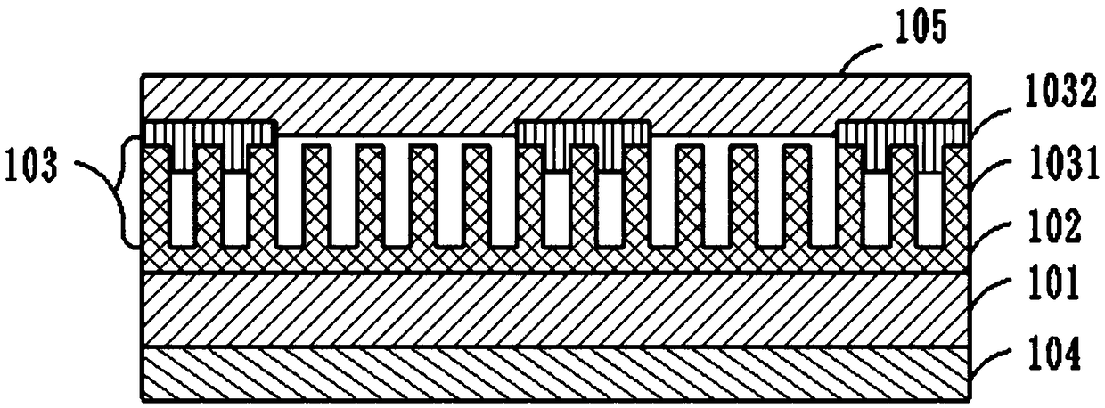
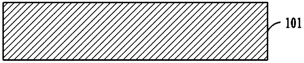
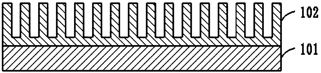
[0028] In order to make the purpose, technical solutions and advantages of the embodiments of the present invention clearer, the technical solutions in the embodiments of the present invention will be clearly and completely described below in conjunction with the drawings in the embodiments of the present invention. Obviously, the described embodiments It is a part of the embodiments of the present invention, rather than all embodiments; based on the embodiments of the present invention, all other embodiments obtained by those of ordinary skill in the art without creative work, all belong to the protection scope of the present invention .

[0029] Secondly, the present invention is described in detail in combination with schematic diagrams. When describing the embodiments of the present invention in detail, for the convenience of explanation, the cross-sectional view showing the device structure will not be partially enlarged according to the general scale, and the schematic di...


PUM


Abstract

The invention provides a silicon carbide material-based Schottky micro nuclear battery. The battery comprises a silicon carbide single crystal substrate, a silicon carbide one-dimensional nanowire array, a Schottky contact electrode, an ohmic contact electrode and a radioactive source layer; the silicon carbide one-dimensional nanowire array is located on the front surface of the silicon carbide single-crystal substrate; the silicon carbide one-dimensional nanowire array is provided with an N-type doped region; the Schottky contact electrode includes a barrier metal layer and an N-type doped region; the surface of the barrier metal layer is interdigital; the ohmic contact electrode is located on the back surface of the silicon carbide single-crystal substrate; and the radioactive source layer is located on the barrier metal layer. The micro nuclear battery provided by the invention has the advantages of novel and reasonable structure, high energy conversion efficiency and low production cost, and is suitable for the field of semiconductor micro devices.

Description

technical field [0001] The invention relates to the technical field of semiconductor micro-devices, in particular to a Schottky micro-nuclear battery based on silicon carbide material and a preparation method thereof. Background technique [0002] A micronuclear battery is a device that converts particle energy (such as alpha particles, beta particles, and gamma rays) emitted by the decay of radioactive isotopes into electrical energy by using semiconductor diodes as an energy conversion structure. Usually, micronuclear batteries use the ionization effect of radiation particles emitted by radioactive isotopes in semiconductor materials as energy sources, and collect electron-hole pairs generated by radiation particles in semiconductors to generate output power. It has the advantages of high energy density, small size, long life, good working stability and easy integration, and its energy conversion structure is simple, the processing technology is mature, and it has broad de...

Claims


Application Information

Patent Timeline
IPC IPC(8): G21H1/06
CPCG21H1/06
Inventor 刘红梅尉国栋
Owner SHANXI DATONG UNIV
Why Eureka
Try Eureka