Semiconductor structures and methods of forming them

A technology of semiconductor and gate structure, which is applied in the field of semiconductor structure and its formation, can solve the problems of increased difficulty in the manufacturing process of fin field effect transistors, poor performance of fin field effect transistors, and decreased reliability, so as to reduce the risk of missing , Improve production yield and device reliability, and ensure the effect of product yield

Active Publication Date: 2021-06-08
SEMICONDUCTOR MANUFACTURING INTERNATIONAL (BEIJING) CORP +1
View PDF4 Cites 0 Cited by
  • Summary
  • Abstract
  • Description
  • Claims
  • Application Information

AI Technical Summary

Problems solved by technology

[0005] However, as the density of semiconductor devices increases and the size shrinks, the manufacturing process of fin field effect transistors becomes more difficult, and the performance and reliability of the formed fin field effect transistors deteriorate.

Method used


Image

  • Semiconductor structures and methods of forming them
  • Semiconductor structures and methods of forming them
  • Semiconductor structures and methods of forming them

Examples


Embodiment Construction

[0032] As mentioned in the background art, as the density of semiconductor devices increases and the size shrinks, the performance and reliability of the formed fin field effect transistors deteriorate.

[0033] During the etching process for removing the dummy gate oxide layer, the isolation layer at the bottom of the first opening is etched simultaneously, which increases the risk of a short circuit between the gate and the source region or the drain region. As the size of the FinFET becomes smaller, the risk of the short circuit is greater, and the influence on the reliability of the device is more obvious. It will be described below in conjunction with the accompanying drawings.

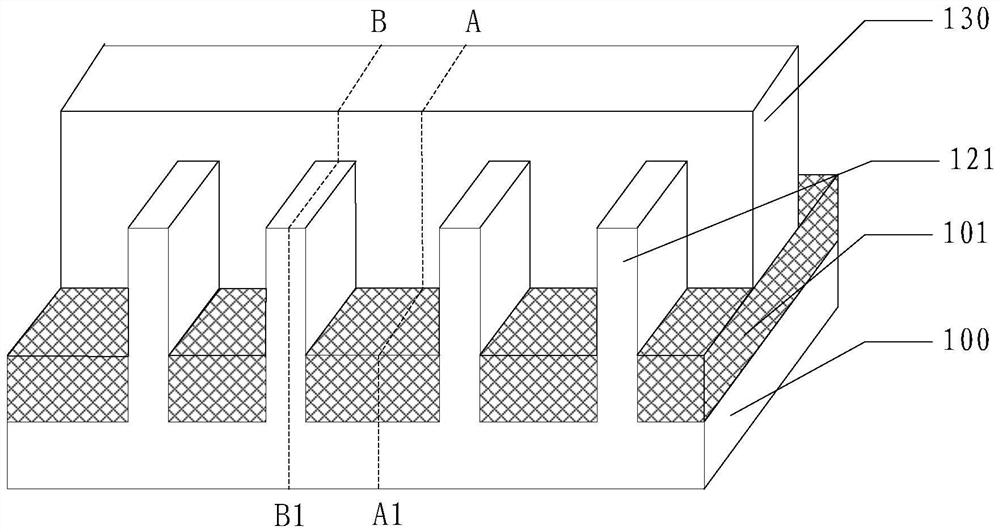
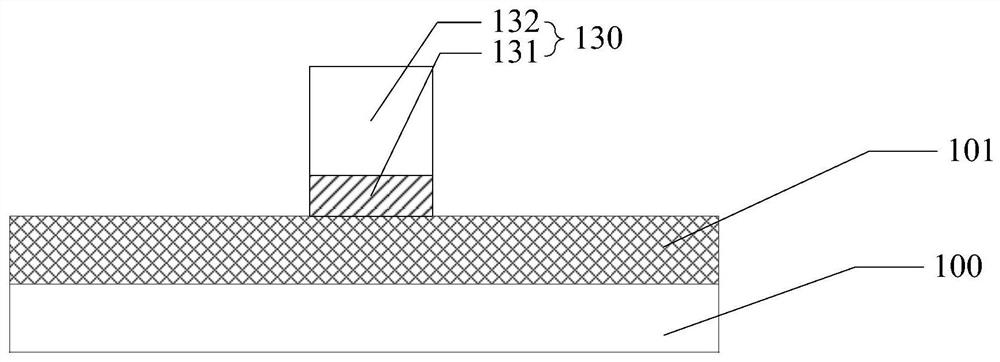
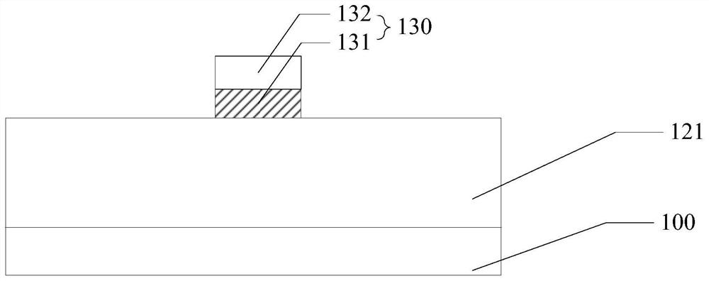
[0034] Figure 1 to Figure 6 It is a structural schematic diagram of each step of a method for forming a semiconductor structure.

[0035] Please refer to figure 1 , figure 2 and image 3 , figure 1 is a schematic diagram of the local three-dimensional structure, figure 2 for figure 1...


PUM

PropertyMeasurementUnit
thicknessaaaaaaaaaa

Abstract

The present invention provides a semiconductor structure and a forming method thereof, wherein the forming method includes: providing a substrate, forming a second isolation layer and a first isolation layer, and forming a first side wall on a side wall of the first isolation layer; A source region and a drain region are formed outside the first spacer; the dummy gate structure is removed, a first opening is formed in the dielectric structure, and the gate structure is filled in the first opening. The forming method prevents a short circuit between the gate and the source region or the drain region located outside the first spacer, thereby improving the production yield and device reliability of the semiconductor structure.

Description

technical field [0001] The invention relates to the technical field of semiconductor manufacturing, in particular to a semiconductor structure and a forming method thereof. Background technique [0002] With the rapid development of semiconductor manufacturing technology, semiconductor devices are developing towards higher element density and higher integration. Transistors, as the most basic semiconductor devices, are being widely used at present. The control ability of traditional planar transistors on channel current is weakened, resulting in short channel effect and leakage current, which ultimately affects the electrical performance of semiconductor devices. [0003] In order to overcome the short channel effect of the transistor and suppress the leakage current, the prior art proposes a fin field effect transistor (Fin FET), which is a common multi-gate device, and the structure of the fin field effect transistor includes : the fin and the dielectric layer located on ...

Claims


Application Information

Patent Timeline
Patent Type & Authority Patents(China)
IPC IPC(8): H01L21/336H01L29/78
CPCH01L29/66545H01L29/66795H01L29/785
Inventor 周飞
Owner SEMICONDUCTOR MANUFACTURING INTERNATIONAL (BEIJING) CORP
Why Eureka
Try Eureka