A method for improving white pixels of a CIS by optimizing a SAB process

A white pixel, oxide layer technology, applied in radiation control devices, electrical components, electrical solid devices, etc., can solve the problem of reducing white pixels and so on

Inactive Publication Date: 2018-12-21
SHANGHAI HUALI MICROELECTRONICS CORP
View PDF4 Cites 2 Cited by
  • Summary
  • Abstract
  • Description
  • Claims
  • Application Information

AI Technical Summary

Problems solved by technology

[0005] The present invention proposes a method for improving CIS white pixels by optimizing the SAB process to improve the problem of metal pollution, thereby improving the stability of CIS devices and reducing white pixels

Method used


Image

  • A method for improving white pixels of a CIS by optimizing a SAB process

Examples


Embodiment Construction

[0022] The specific embodiments of the present invention are given below in conjunction with the accompanying drawings, but the present invention is not limited to the following embodiments. Advantages and features of the present invention will be apparent from the following description and claims. It should be noted that all the drawings are in very simplified form and use imprecise ratios, which are only used for the purpose of conveniently and clearly assisting in describing the embodiments of the present invention.

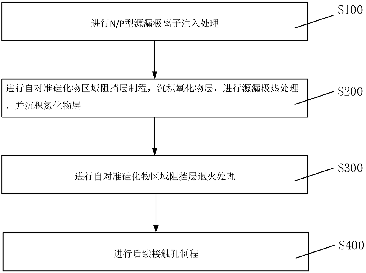
[0023] Please refer to figure 1 , figure 1 Shown is a flowchart of a method for improving CIS white pixels in a preferred embodiment of the present invention. The present invention proposes a method for improving CIS white pixels by optimizing the SAB process, comprising the following steps:

[0024] Step S100: performing N / P type source-drain ion implantation treatment;

[0025] Step S200: performing a salicide region barrier layer process, depositing an ...


PUM

PropertyMeasurementUnit
thicknessaaaaaaaaaa
thicknessaaaaaaaaaa

Abstract

The invention provides a method for improving CIS white pixels by optimizing a SAB manufacturing process, which comprises the following steps that N/P type source-drain ion implantation treatment is carried out; A manufacture process of a self-aligned silicide region barrier layer is carried out, an oxide layer is deposited, a source-drain heat treatment is carried out, and a nitride layer is deposited; The self-aligned silicide region barrier layer is annealed; and a subsequent contact hole proces is performed. The invention can simply and effectively improve metal pollution through thin filmdeposition and annealing process, and does not involve other effects. The invention reduces the white pixels of a CIS device, reduces dark current of the CIS device, and does not affect other parameters.

Description

technical field [0001] The invention relates to the field of semiconductor integrated circuit manufacturing, and in particular to a method for improving CIS white pixels by optimizing the SAB process. Background technique [0002] Since Bell Laboratories in the United States proposed the concept of solid-state imaging devices in the late 1960s, solid-state image sensors have developed rapidly and become an important branch of sensing technology. It is an indispensable peripheral for personal computer multimedia, and also a core device in monitoring equipment. In recent years, due to the improvement of integrated circuit design technology and process level, CIS (CMOS IMAGE SENSOR, Complementary Metal Oxide Semiconductor Image Sensor), that is, CMOS image sensor due to its inherent features such as intra-pixel amplification, column parallel structure, high integration , Single power supply and low voltage power supply, low cost and low technical threshold have been widely use...

Claims


Application Information

Patent Timeline
Patent Type & Authority Applications(China)
IPC IPC(8): H01L27/146
CPCH01L27/14692H01L27/14698
Inventor 范洋洋王明
Owner SHANGHAI HUALI MICROELECTRONICS CORP
Why Eureka
Try Eureka