Preparation method of GaN-based HEMT gold-free ohmic contact electrode based on TiN
A technology of ohmic contact electrodes and source-drain electrodes, which is applied to circuits, electrical components, metal material coating processes, etc., to achieve the effects of reducing process temperature and process complexity, reducing manufacturing costs, and improving compatibility
- Summary
- Abstract
- Description
- Claims
- Application Information
AI Technical Summary
Problems solved by technology
Method used
Image
Examples
Embodiment 1
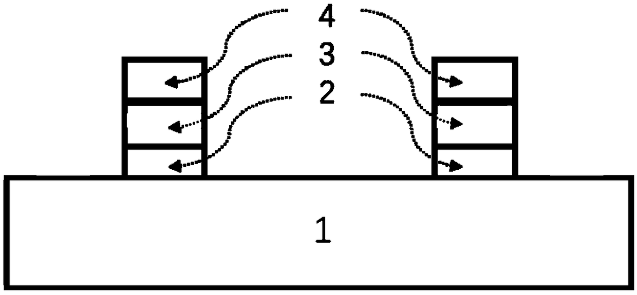
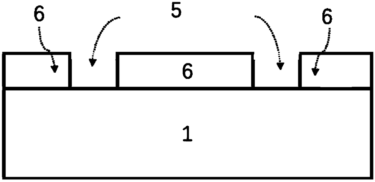
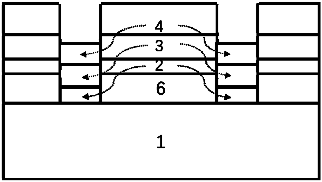
[0034] Such as Figure 1 ~ Figure 3 Shown, a kind of preparation method of GaN-based HEMT without gold ohmic contact electrode based on TiN, the steps are as follows:
[0035] Step 1, source-drain electrode pattern. A gold-free source-drain electrode pattern region 5 is defined on the GaN-based epitaxial layer 1 by a photolithography process, and a photolithography mask 6 covers areas other than the gold-free source-drain electrode pattern region 5 on the GaN-based epitaxial layer 1, such as figure 2 shown.
[0036] Step two, surface treatment. Surface treatment is performed on the source-drain electrode pattern area 5, and the surface oxide at the source-drain electrode pattern 5 is cleaned with dilute hydrochloric acid solution;
[0037]Step 3, depositing electrode materials. The gold-free source-drain electrode metal layer is deposited by magnetron sputtering. Specifically, the gold-free source-drain electrode metal layer is Ti metal sputtered on the surface of the sam...
Embodiment 2
[0043] Step 1, source-drain electrode pattern. A gold-free source-drain electrode pattern region 5 is defined on the GaN-based epitaxial layer by photolithography, and a photolithographic mask 6 covers the GaN-based epitaxial layer 1 except for the gold-free source-drain electrode pattern region 5 .
[0044] Step two, surface treatment. Surface treatment is performed on the source-drain electrode pattern area 5, and the surface oxide at the source-drain electrode pattern area 5 is cleaned with dilute hydrochloric acid solution;
[0045] Step 3, depositing electrode materials. The gold-free source-drain electrode metal layer is deposited by magnetron sputtering. Specifically, the gold-free source-drain electrode metal layer is Ti metal sputtered on the surface of the sample prepared in step 2 sequentially by magnetron sputtering. 2. Al metal 3 and TiN metal 4 have a thickness of 20nm, 100nm and 100nm respectively, forming a Ti / Al / TiN multilayer metal system. Among them, the ...
Embodiment 3
[0050] Step 1, source-drain electrode pattern. A gold-free source-drain electrode pattern region 5 is defined on the GaN-based epitaxial layer by photolithography, and a photolithographic mask 6 covers the GaN-based epitaxial layer 1 except for the gold-free source-drain electrode pattern region 5 .
[0051] Step two, surface treatment. Surface treatment is performed on the source-drain electrode pattern area 5, and the surface oxide at the source-drain electrode pattern area 5 is cleaned with dilute hydrochloric acid solution;
[0052] Step 4, depositing electrode materials. Deposit the gold-free source-drain electrode metal layer by magnetron sputtering. Specifically, the gold-free source-drain electrode metal layer is the Ti metal 2, Al metal 3 and TiN metal 4 have a thickness of 20nm, 100nm and 100nm respectively, forming a Ti / Al / TiN multilayer metal system. Among them, the low-temperature magnetron sputtering TiN thin film is deposited by reactive magnetron sputtering,...
PUM
| Property | Measurement | Unit |
|---|---|---|
| Thickness | aaaaa | aaaaa |
Abstract
Description
Claims
Application Information
 - R&D
- Intellectual Property
- Life Sciences
- Materials
- Tech Scout
- Unparalleled Data Quality
- Higher Quality Content
- 60% Fewer Hallucinations
Browse by: Latest US Patents, China's latest patents, Technical Efficacy Thesaurus, Application Domain, Technology Topic, Popular Technical Reports.
© 2025 PatSnap. All rights reserved.Legal|Privacy policy|Modern Slavery Act Transparency Statement|Sitemap|About US| Contact US: help@patsnap.com


