
A novel anti-welding double-sided LED exposure machine

An exposure machine and anti-soldering technology, which is applied in the direction of photomechanical equipment, microlithography exposure equipment, and photolithography exposure equipment, etc., can solve the problem of affecting site space and additional costs for purchasing multiple machines, different images from top to bottom, and the inability to realize four-dimensional Problems such as pairwise alignment of faces

Pending Publication Date: 2018-12-18
东莞市多普光电设备有限公司
View PDF0 Cites 2 Cited by
  • Summary
  • Abstract
  • Description
  • Claims
  • Application Information

AI Technical Summary

Problems solved by technology

[0002] In the field of PCB manufacturing equipment, the image transfer process mainly includes inner layer, outer layer, and solder mask. At present, the process of inner layer and outer layer is mature for double-sided exposure, but for the solder mask process, the traditional one-side exposure or Use a fully automatic exposure machine to expose on both sides successively (it is also a 180-degree flip operation with a flipper in the middle of the two exposure machines). The technical difficulty of double-sided exposure in the solder mask process is alignment inspection. If double-sided exposure is used, PCB boards are required. The images on both sides are respectively aligned with the upper and lower frames. Most of the existing PCB board alignment is to align the upper and lower frames, and then align the upper and lower images of the PCB with the lower frame. Because the upper and lower graphics of the PCB are transferred in the previous process equipment images There will always be a certain manufacturing error, which will cause the upper and lower images of the PCB itself to be different, and then it will not be possible to achieve two-to-two alignment of the four sides, resulting in the solder mask process can only be carried out on one side, so only the purchase of double semi-automatic and fully automatic solder mask Exposure machine or LDI to match the output of the previous process, which seriously affects the site space and the additional cost of purchasing more machines

Method used


Image

  • A novel anti-welding double-sided LED exposure machine
  • A novel anti-welding double-sided LED exposure machine
  • A novel anti-welding double-sided LED exposure machine

Examples


Embodiment Construction

[0016] In order to enable those skilled in the art to better understand the technical solutions of the present invention, the present invention will be described in detail below with reference to the accompanying drawings. The description in this section is only exemplary and explanatory, and should not have any limiting effect on the protection scope of the present invention. .

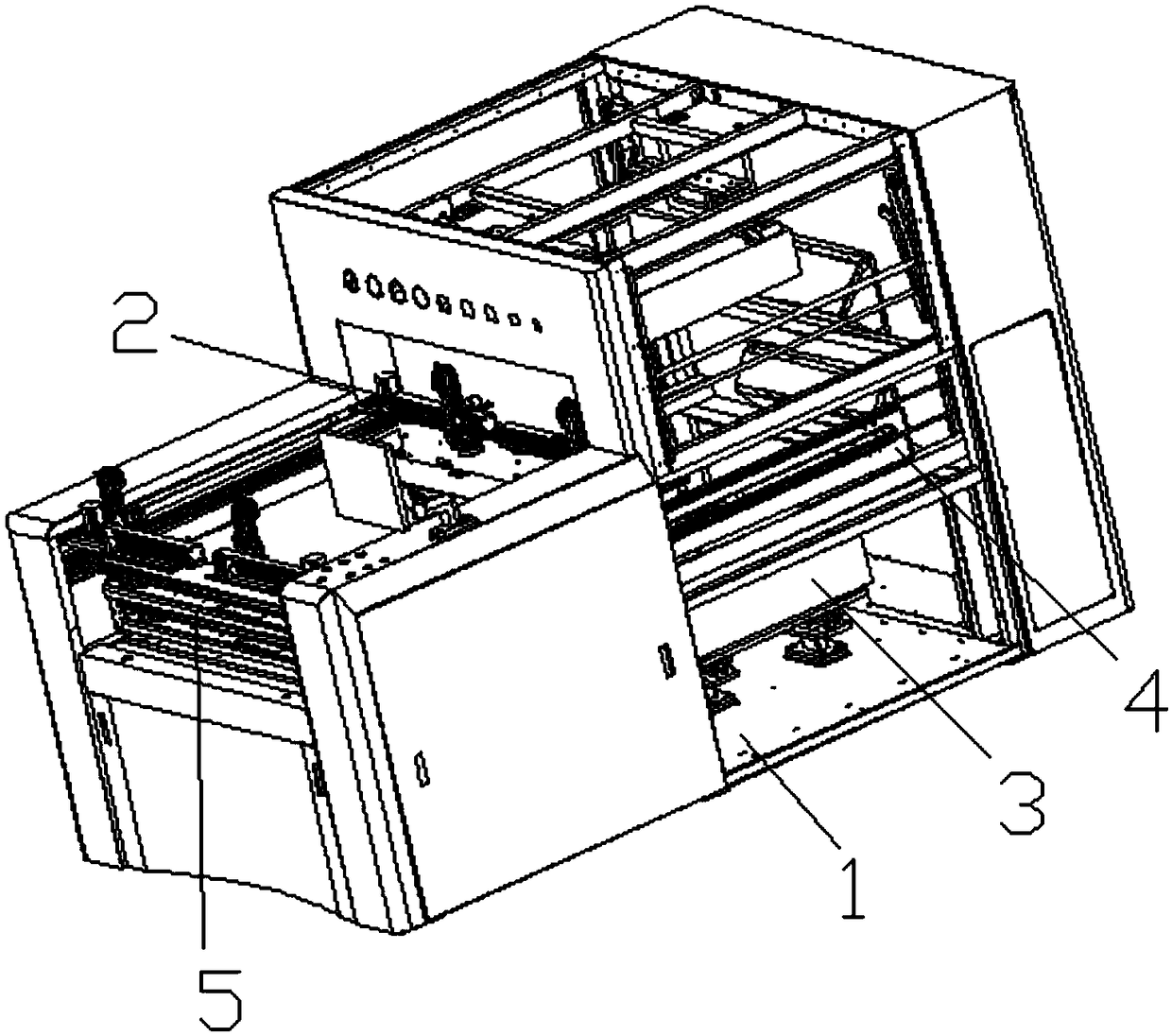
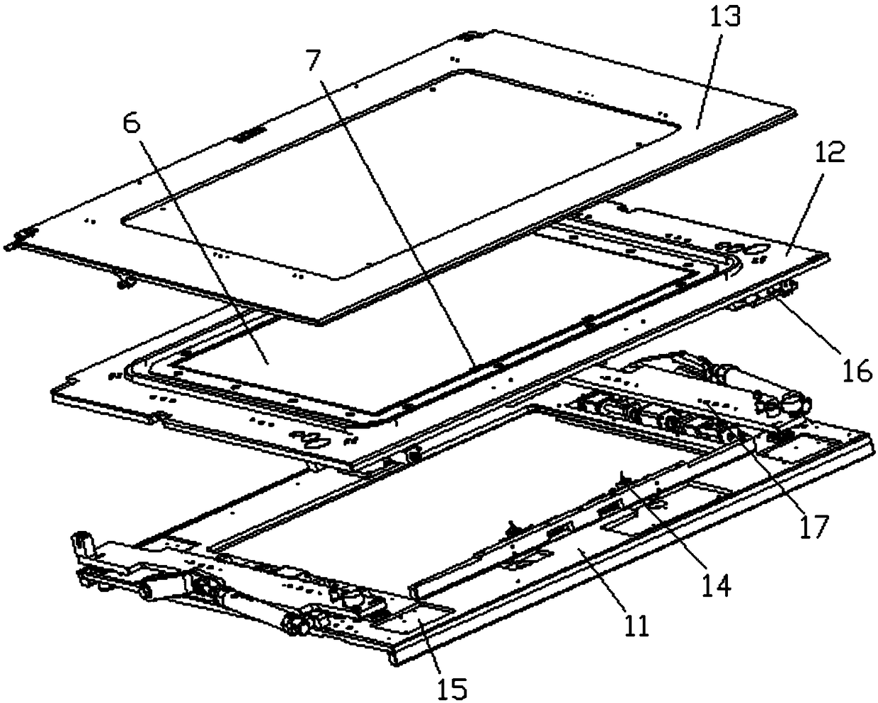
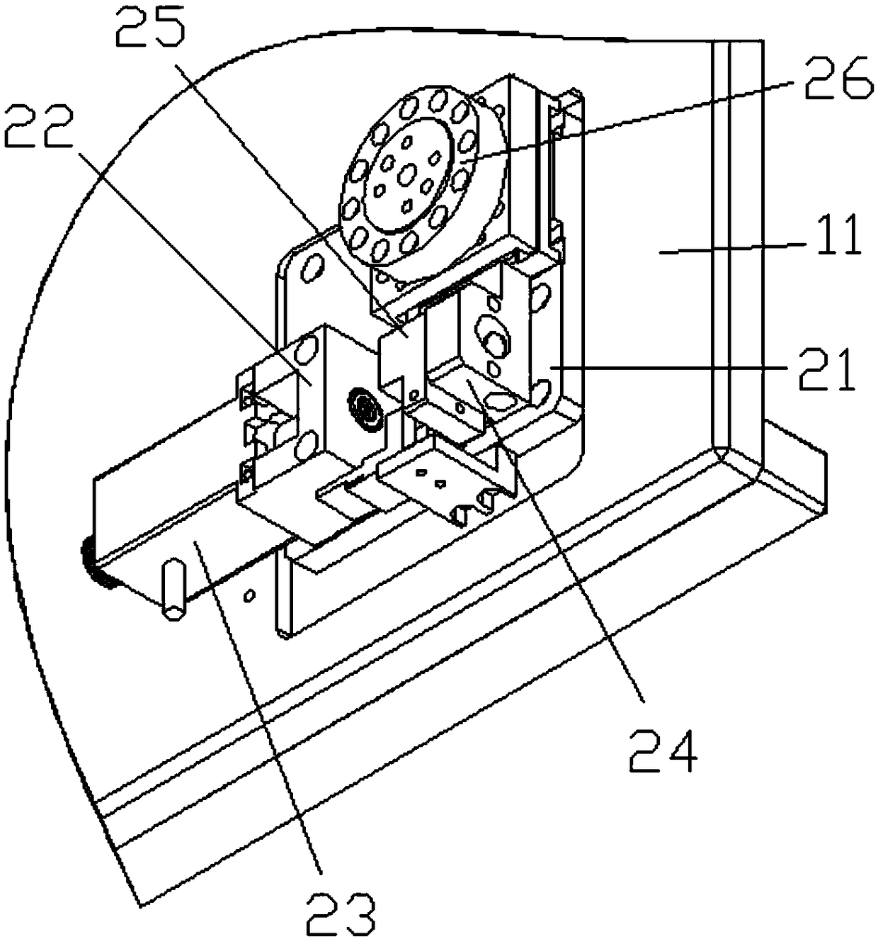
[0017] Such as Figure 1-Figure 2 As shown, the specific structure of the present invention is: a new type of welding-resistant double-sided LED exposure machine, comprising a frame 1 and a conveying slide 4, and the conveying slide 4 is matched with a frame 5, which is characterized in that the The rack 1 is located on the upper and lower parts of the conveying slide 4 and is provided with an LED light source 3. The frame 5 includes a lower frame 11 that cooperates with the conveying slide 4, and the lower frame 11 is hinged with an upper frame 13, so The lower frame 11 is provided with a middle frame ...


PUM


Abstract

The invention relates to a novel anti-welding double-sided LED exposure machine, including the frame and conveyor rails, the conveying slide rail is fitted with a frame, characterized by, the machineframe is arranged at the upper and lower parts of the conveying slide rail and is provided with an LED lamp source, the frame includes a lower frame that cooperates with the conveyor rail, the lower frame is hinged with an upper frame, the lower frame is provided with a middle frame which bears the product, and the lower part of the middle frame is provided with a PIN positioning device which is matched with the alignment hole on the middle frame and the product, the lower frame is provided with an alignment device capable of making the middle frame movable, An object of the present inventionis to provide a novel anti-welding double-sided LED exposure machine, A 3-layer frame is adopt, that upper image of the PCB is aligned with the middle frame image through a PIN position device, the middle frame is moved through the aligning device, the low image of the PCB board is aligned with the upper frame image, two or two alignments of the four images are realized, and the welding-proof double-sided LED exposure can be realized, the processing efficiency is improved, and the cost is reduced.

Description

Technical field [0001] The invention relates to the technical field of exposure machines for PCB manufacturing boards, in particular to a new type of solder-resistant double-sided LED exposure machine. Background technique [0002] In the field of PCB manufacturing board manufacturing equipment, the image transfer process mainly includes inner layer, outer layer, and solder mask. At present, the inner layer and outer layer processes are mature for double-sided exposure, but the traditional solder mask process is still single-sided exposure or Use a fully automatic exposure machine to expose on both sides one after the other (also in the middle of the two exposure machines with a plate turning machine to turn 180 degrees), the technical difficulty of the double-sided exposure of the solder mask process is the alignment check. If double-sided exposure is used, a PCB board is required The images on the two sides are aligned with the upper and lower frames respectively. Most of the e...

Claims


Application Information

Patent Timeline
Patent Type & Authority Applications(China)
IPC IPC(8): G03F7/20H05K3/28
CPCH05K3/282G03F7/20G03F7/2032
Inventor 陈振才柯华廉
Owner 东莞市多普光电设备有限公司
Learn More