
Patsnap Eureka
For R&D, Patsnap Eureka makes reading and utilizing patents & technical documents easy.
Patsnap Eureka AIR
Designed for self-driven R&D workflows. Generate viable solutions, solve complex R&D challenges, empower your innovation with AI.

Patsnap Eureka Materials
Designed for material experts only. Revolutionize your material R&D, from search, analyze, to developing new materials.

TechResearch
Generate reliable direction feasibility study reports for your R&D in just a few steps.

TechSeek
Discover and master advanced knowledge NOW. Basics, ideas, possibilities, all at once.

TechMind
As an expert in R&D Theories, TechMind can generates customized viable solutions instantly.

TechRisk
Analyze your overall solution with one click, know your potential R&D risks in advance.

TechMonitor
Get weekly tech updates, stay abreast of the latest tech innovations and key insights.
Semiconductor structure
A technology of semiconductor and stacked structure, applied in the direction of semiconductor devices, electrical solid devices, electrical components, etc., can solve the problems of large stress on the substrate, affecting the performance of the memory, and prone to voids, etc., to reduce the possibility of warping , reduced strain, and reduced grain size
- Summary
- Abstract
- Description
- Claims
- Application Information
AI Technical Summary
Problems solved by technology
Method used
Image

Examples
Embodiment Construction
[0021] A semiconductor structure proposed by the present invention and its preparation method will be described in detail below with reference to the accompanying drawings and specific embodiments.
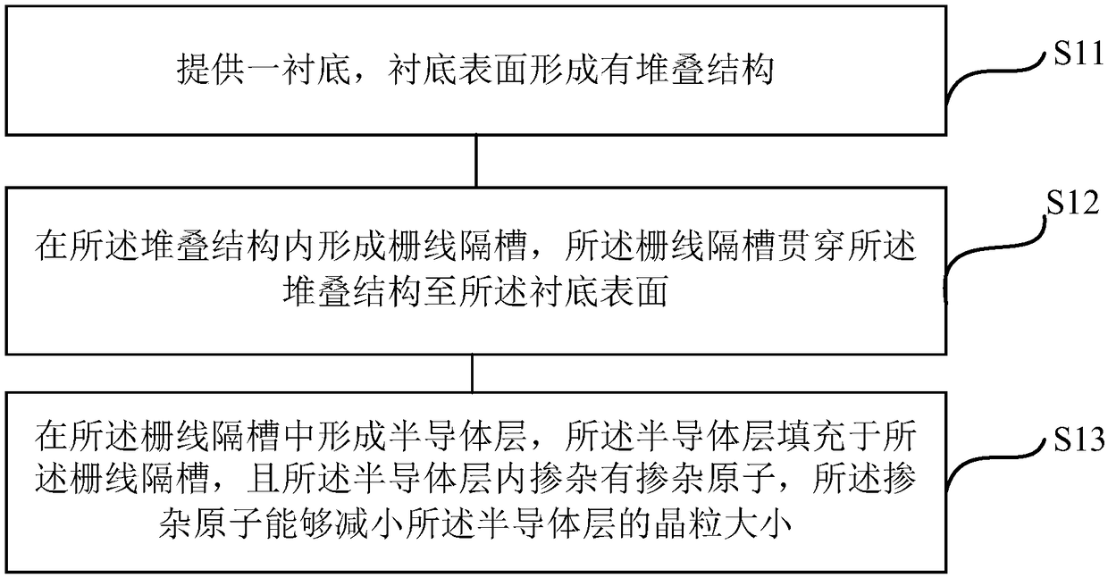
[0022] see figure 1 , is a flow chart of the method for preparing the semiconductor structure in a specific embodiment. The manufacturing method of the semiconductor structure includes the following steps: S11: providing a substrate, and a stack structure is formed on the surface of the substrate. S12: Forming a gate line spacer in the stack structure, the gate line spacer penetrating through the stack structure to the surface of the substrate. S13: forming a semiconductor layer in the gate line spacer, the semiconductor layer is filled in the gate line spacer, and the semiconductor layer is doped with dopant atoms, and the dopant atoms can reduce the The grain size of the semiconductor layer.
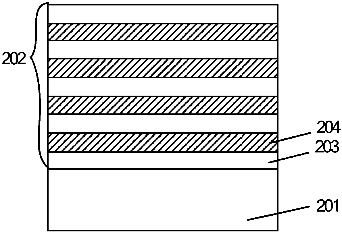
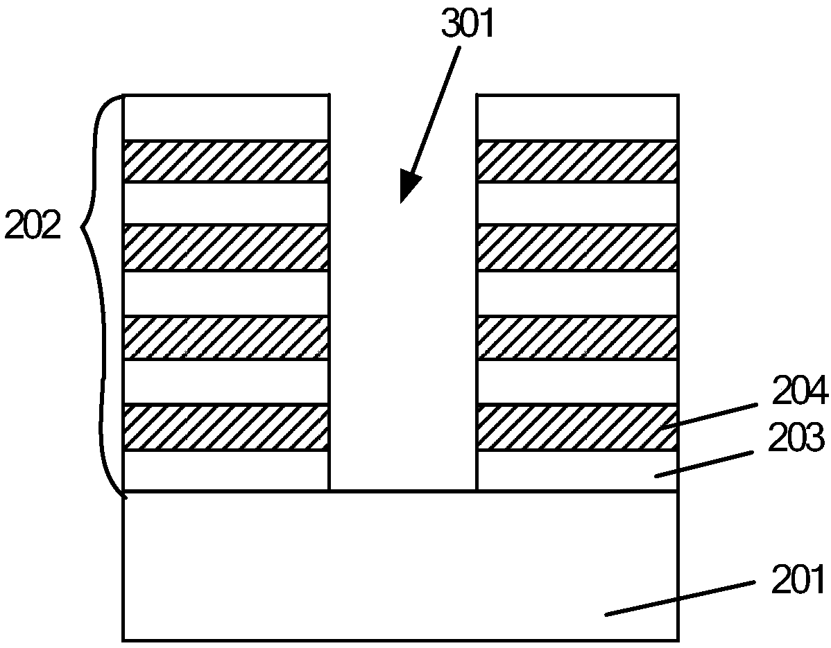
[0023] see Figure 2 to Figure 6 , is a structural schematic diagram of a process ...
PUM
 Abstract
Description
Claims
Application Information
 - R&D Engineer
- R&D Manager
- IP Professional
- Industry Leading Data Capabilities
- Powerful AI technology
- Patent DNA Extraction
Browse by: Latest US Patents, China's latest patents, Technical Efficacy Thesaurus, Application Domain, Technology Topic, Popular Technical Reports.
© 2024 PatSnap. All rights reserved.Legal|Privacy policy|Modern Slavery Act Transparency Statement|Sitemap|About US| Contact US: help@patsnap.com