
A semiconductor wafer dicing machine

A dicing machine and semiconductor technology, used in semiconductor/solid-state device manufacturing, working accessories, electrical components, etc., can solve the problems of clogging of adsorption holes, inability to adjust the size of adsorption pore size, low adaptability, etc., to avoid powder clogging. Effect

Active Publication Date: 2020-08-25
河北擎越电子科技有限公司
View PDF18 Cites 1 Cited by
  • Summary
  • Abstract
  • Description
  • Claims
  • Application Information

AI Technical Summary

Problems solved by technology

[0005] This technical solution can improve the adsorption stability and reliability of the wafer, but it still has the following defects. The size of the adsorption aperture cannot be adjusted, making its adaptability low. weaken

Method used


Image

  • A semiconductor wafer dicing machine
  • A semiconductor wafer dicing machine
  • A semiconductor wafer dicing machine

Examples


Embodiment approach

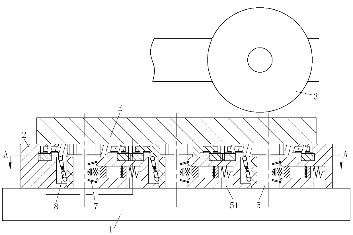
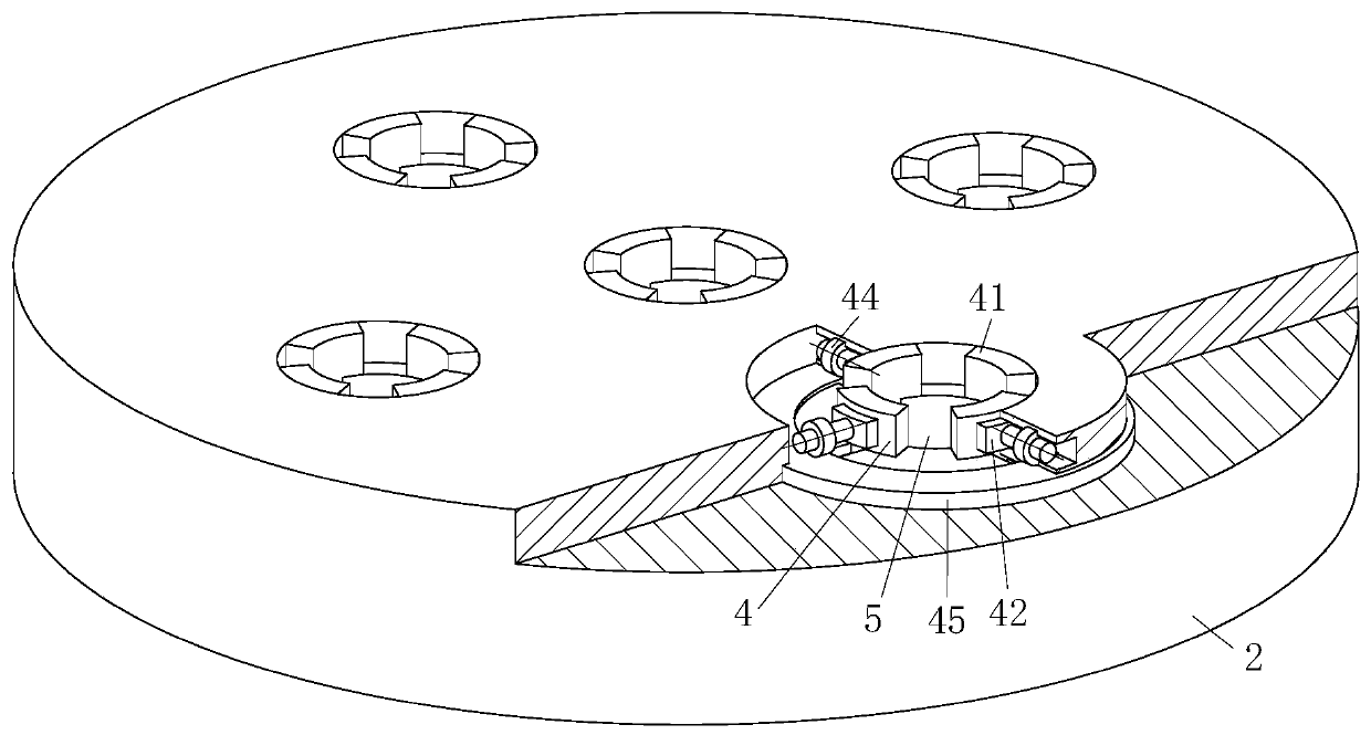
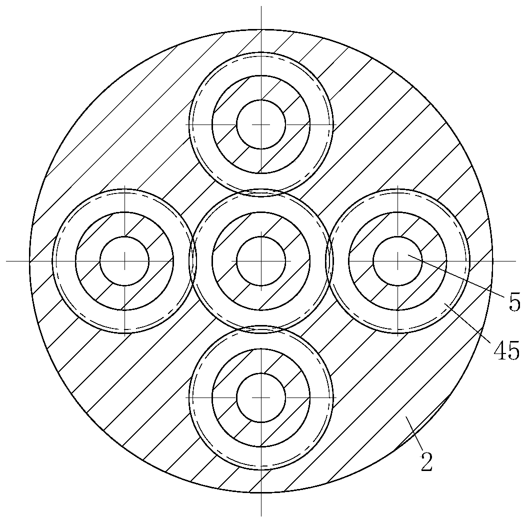
[0028] As an embodiment of the present invention, one side of the adsorption hole 5 is provided with a communication hole 51; one end of the communication hole 51 communicates with the adsorption hole 5; the other end of the communication hole 51 communicates with the outside world; the communication hole 51 A dredging block 52 is slidingly installed inside; the dredging block 52 is provided with a No. 1 through hole 53 in the same direction as the adsorption hole 5 , and the dredging block 52 is used to prevent the adsorption hole 5 from being blocked. When working, after the adsorption hole 5 absorbs the wafer, the communication hole 51 is always connected with the outside world. When the suction hole 5 is vacuumed, the external air pressure pushes the dredging block 52 to move into the adsorption hole 5. After the wafer cutting is completed, the dredging The block 52 returns under the action of the spring, so as to alleviate the blockage of the cutting dust to the adsorption...


PUM


Abstract

The invention belongs to the technical field of semiconductor production, in particular to a semiconductor wafer scriber. The semiconductor wafer scriber comprises a workbench, a sucking disc, a vacuum generator and a cutting knife, wherein the vacuum generator is arranged in the workbench, the sucking disc is arranged on the workbench and is used for adsorbing a wafer, and the cutting knife is arranged above the sucking disc. The semiconductor wafer scriber further comprises an adjustment device, and the adjustment device is arranged on an adsorption hole of the sucking disc and is used for adjusting the adsorption area of the adsorption hole. The semiconductor wafer scriber changes the size of the adsorption hole by the adjustment device, thereby preventing the adsorption hole from beingtoo small so as to cause insufficient adsorption force and cutting damage and affect the quality of the wafer. A communicating hole is formed in one side of the adsorption hole, and a dredging blockis arranged in the communicating hole in a sliding mode. After the inner part of the adsorption hole is vacuumized, outside air pressure pushes the dredging block to move into the adsorption hole. After the wafer is cut, the dredging block returns under the action of a spring to ease the blockage of the adsorption hole by cutting powdered scraps.

Description

technical field [0001] The invention belongs to the technical field of semiconductor production, in particular to a semiconductor wafer dicing machine. Background technique [0002] During the dicing process of the dicing machine, the wafer needs to be fixed on the suction cup when dicing. A suction groove is processed on the surface of the suction cup, and the wafer is adsorbed on the surface of the suction cup by generating a low-pressure vacuum in the suction groove. Due to the high-speed rotation of the spindle during the scribing process, the blade generates a large cutting force when scribing the wafer, so the adsorption of the wafer needs to be very stable and reliable. However, the existing suction cups have the problem of poor adsorption stability. [0003] The size of the adsorption force of the suction cup will directly affect the stability of the vacuum adsorption, and the size of the adsorption force is related to the size, shape and layout of the adsorption g...

Claims


Application Information

Patent Timeline
Patent Type & Authority Patents(China)
IPC IPC(8): B28D5/00B28D7/04H01L21/683H01L21/67
CPCB28D5/0011B28D5/0094H01L21/67092H01L21/6838
Inventor 李涵潘万胜
Owner 河北擎越电子科技有限公司
Learn More