Silicon wafer etching apparatus

An etching device and a technology for silicon wafers, which are applied in the fields of electrical components, semiconductor/solid-state device manufacturing, circuits, etc., can solve the problems of low etching precision of wafers, inability to achieve batch etching, and uneven etching of wafers, etc. problems, to achieve the effect of fast etching speed, improved precision, and uniform etching

Active Publication Date: 2018-10-19
苏州因知成新能源有限公司
View PDF5 Cites 0 Cited by
  • Summary
  • Abstract
  • Description
  • Claims
  • Application Information

AI Technical Summary

Problems solved by technology

However, the precision of the technical solution for wafer etching is not high, and the etching of the wafer is uneven, which affects the quality of the product, cannot achieve batch etching, and the etching efficiency is slow

Method used


Image

  • Silicon wafer etching apparatus
  • Silicon wafer etching apparatus
  • Silicon wafer etching apparatus

Examples


Embodiment Construction

[0024] In order to make the technical means, creative features, goals and effects achieved by the present invention easy to understand, the present invention will be further described below in conjunction with specific embodiments.

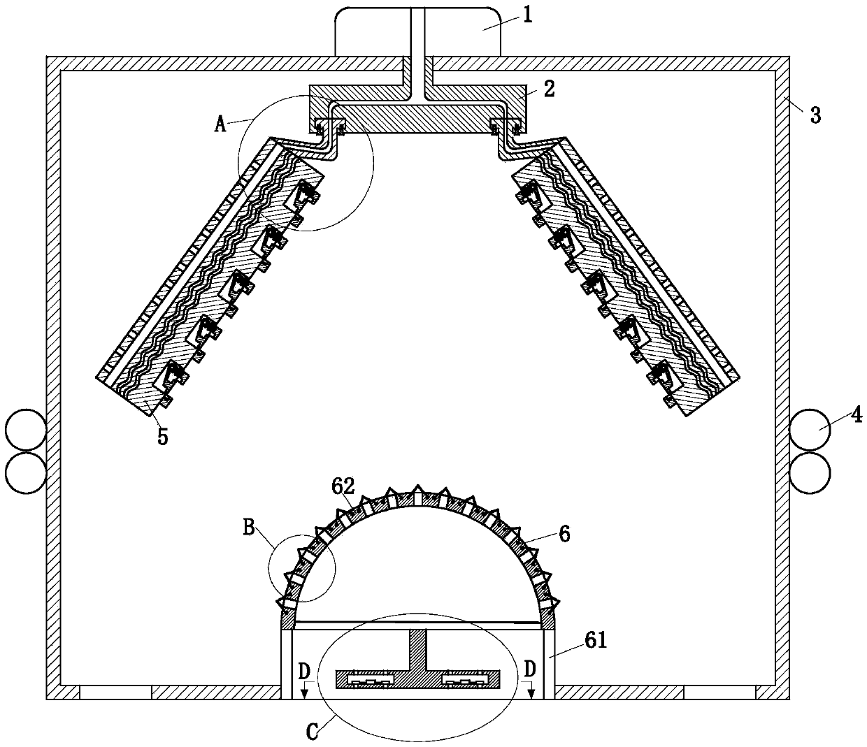
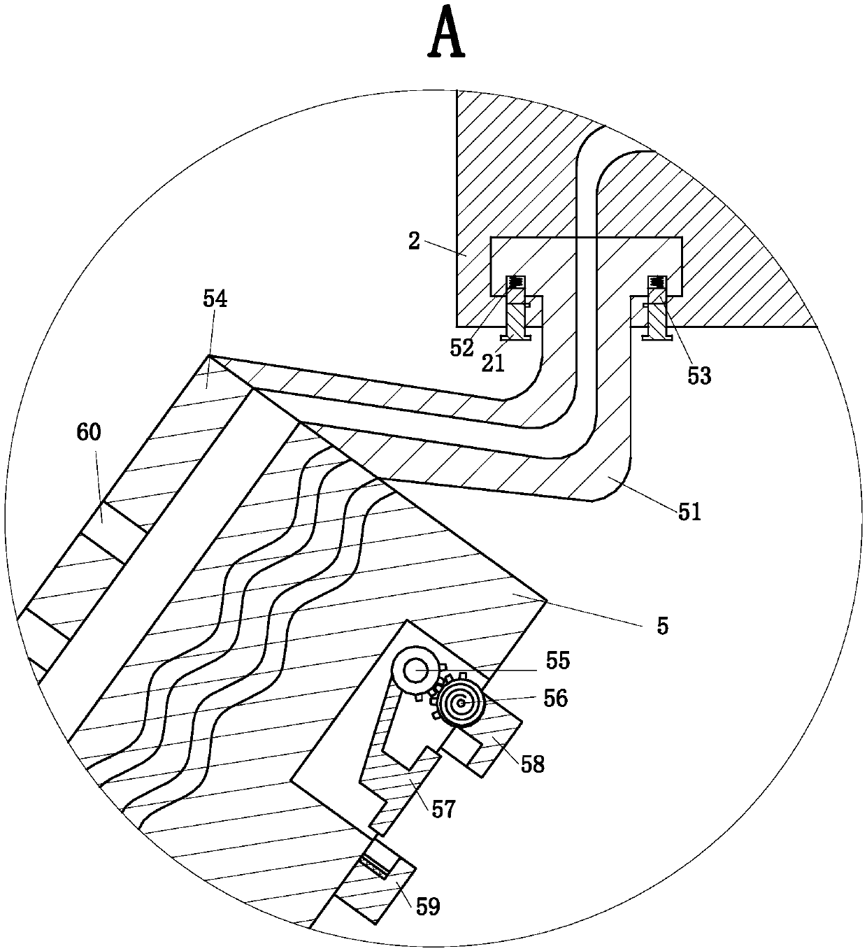
[0025] Such as Figure 1 to Figure 5 As shown, a silicon wafer etching device according to the present invention includes a motor 1, a turntable 2, a housing 3 and an excitation coil 4, and also includes a wafer fixing module 5 and a gas injection module 6. The motor 1 Installed directly above the housing 3; the turntable 2 is installed on the motor shaft of the motor 1; the excitation coil 4 surrounds the outer ring of the housing 3; the wafer fixing module 5 is installed on the turntable 2 Below, the wafer fixing module 5 is used for fixing the wafer and introducing dry hot air; corrosive gas.

[0026] As an embodiment of the present invention, the turntable 2 is provided with channels, the number of which is four, the turntable 2 is also prov...


PUM


Abstract

The invention belongs to the technical field of semiconductors and specifically relates to a silicon wafer etching apparatus comprising an electric mot, a rotating disk, a housing, an excitation wirecoil, a wafer fixing module and a gas injection module, wherein the electric motor is mounted right above the housing, the rotating disk is mounted on an electric motor shaft of the electric motor, the excitation wire coil surrounds an outer ring of the housing, the wafer fixing module is mounted below the rotating disk, the wafer fixing module is used for fixing wafers and letting in dry hot air,the gas injection module is mounted on a bottom part of the housing, and the gas injection module is used for introducing etching gas into the housing The apparatus disclosed in the invention is mainly used for etching the wafers in batch; the apparatus is high in etching efficiency, great in batch etching speed, adjustable in etching gas direction, high in etching precision and great in etchinguniformity; product quality can be improved.

Description

technical field [0001] The invention belongs to the technical field of semiconductors, in particular to a silicon wafer etching device. Background technique [0002] Etching technique is a technique for selectively etching or stripping the surface of the semiconductor substrate or the surface covering film according to the mask pattern or design requirements in the semiconductor process. Etching technology is not only the basic manufacturing process of semiconductor devices and integrated circuits, but also applied to the processing of thin film circuits, printed circuits and other fine graphics. Etching can also be divided into wet etching and dry etching. Dry etching basically includes two etching mechanisms: ion-bombardment and chemical reaction. Those who deviate from the particle bombardment effect use argon gas (argon), and the lateral erosion of the processed edge is minimal. For partial chemical reaction effects, fluorine-based or chlorine-based gases (such as car...

Claims


Application Information

Patent Timeline
Patent Type & Authority Applications(China)
IPC IPC(8): H01L21/67H01L21/683
CPCH01L21/67017H01L21/67069H01L21/67103H01L21/683
Inventor 徐亚琴李保振
Owner 苏州因知成新能源有限公司
Why Eureka
Try Eureka