Micro solder joint thermal migration test method

A test method and thermal migration technology, applied in the direction of thermal development of materials, can solve the problems of complex production, high cost, incomparability of thermal migration reliability data, etc., and achieve the effect of simple process and low cost

Inactive Publication Date: 2018-10-16
BEIJING UNIV OF TECH
View PDF5 Cites 5 Cited by
  • Summary
  • Abstract
  • Description
  • Claims
  • Application Information

AI Technical Summary

Problems solved by technology

However, the size difference between the two sides of the thermomigration test sample is too large, and the difference between it and the actual solder joint heating area will cause the incomparability of the thermomigration reliability data; some researchers use water cooling at one end of the solder joint to reduce the temperature at one end , forming a temperature difference with the non-water-cooled end to achieve a temperature gradient. However, this structure is complicated to manufacture, high in cost, poor in reproducibility, and difficult to control the temperature gradient, which affects the reliability of the thermal migration experiment.

Method used


Image

  • Micro solder joint thermal migration test method
  • Micro solder joint thermal migration test method
  • Micro solder joint thermal migration test method

Examples


example 1

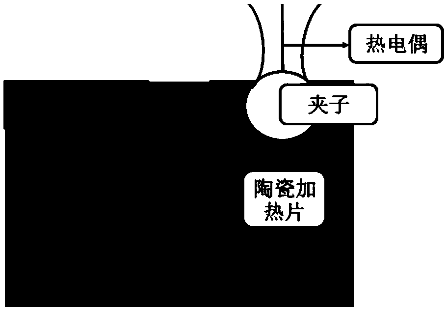
[0023] Combining the following figure 1 , 2 , 3 specifically illustrate the implementation of the present invention.

[0024] 1. Cu pad preparation: the purity is greater than 99.99wt%, and the copper pad is made by wire cutting, and its size is 500μm×2mm×4mm;

[0025] 2. Clean the Cu pad in acetone for 5 minutes, then soak it in the prepared 30vol.% nitric acid aqueous solution for 10 minutes to remove oxides and pollutants on the surface of the Cu pad, and then put it in absolute ethanol Further ultrasonic cleaning, after cleaning and drying for later use;

[0026] 3. Adhere high-temperature-resistant double-sided adhesive on a 10mm×10mm×1.5mm printed circuit board, and place two Cu pads on it with a spacing of 130 μm, and ensure the parallelism of the Cu pads;

[0027] 4. Use a toothpick to fill the Sn0.3Ag0.7Cu solder paste between the two Cu pads, use a hot air reflow soldering machine (Comrade Technology, TN380C) for welding, and cool in the air to obtain Cu / Sn0.3Ag0....

example 2

[0029] Example 2: Combining the following figure 1 , 2 , 4 specifically describe the implementation of the present invention.

[0030] 1. Cu pad preparation: the purity is greater than 99.99wt%, and the copper pad is made by wire cutting, and its size is 500μm×2mm×4mm;

[0031] 2. Put the Cu pad in acetone for 5-10 minutes, then soak it in the prepared 30vol.% nitric acid aqueous solution for a few minutes to remove the oxides and pollutants on the surface of the Cu pad, and then put it into an anhydrous Further ultrasonic cleaning in ethanol, after cleaning, dry for later use;

[0032] 3. Adhere high-temperature-resistant double-sided adhesive on a 10mm×10mm×1.5mm printed circuit board, and place two Cu pads on it with a distance of 200 μm, and ensure the parallelism of the Cu pads;

[0033] 4. Use a toothpick to fill the Sn0.3Ag0.7Cu solder paste between the two Cu pads, use a hot air reflow soldering machine (Comrade Technology, TN380C) for welding, and cool in the air t...


PUM


Abstract

The invention discloses a micro solder joint thermal migration test structure and a production method thereof, and belongs to the field of production and connection of materials. A solder pad for thermal migration test has a raised shape, is adhered to a base plate through a double-faced adhesive tape, a solder paste is filled between two solder pads, the two solder pads are welded to form a solder joint, and the solder joint is polished to form a solder joint for thermal migration test. One ends of the solder pads of the solder joint are heated by ceramic heating pieces, a thermocouple monitors the ceramic heating pieces, a controller is used to control the temperature, and the other ends of the solder pads keep a room temperature state, so two ends of the solder joint have a temperaturedifference, and stable temperature gradient is realized. The temperature controller is arranged to control the temperature of one ends of the solder point solder pads and realize the accurate controlof the temperature difference between two ends of the solder point, so two sides of the solder joint have the controllable temperature gradient, the problem of difficult realization and control of thetemperature gradient in the thermal migration test process of the micro-size solder joint is solved, reliable solder joint thermal migration data is obtained on the premise of the controllable solderjoint temperature gradient, and is evaluated.

Description

technical field [0001] The invention relates to a micro-solder joint thermal migration test method, which belongs to the field of material preparation and connection. A ceramic heating plate and a temperature controller are used to control the temperature gradient at both ends of the solder joint, and is suitable for research on the thermal migration reliability test of the micro-solder joint. This method can effectively guarantee the temperature gradient at both ends of the micro-soldering point, so that reliable soldering point thermal migration data can be obtained and evaluated under the premise that the temperature gradient of the soldering point is controllable. Background technique [0002] Solder joints are an integral part of microelectronic interconnection, playing the role of mechanical connection, electrical signal transmission and heat dissipation. At present, the microelectronic packaging space is reduced, the heat generation of the chip is intensified, and a l...

Claims


Application Information

Patent Timeline
IPC IPC(8): G01N25/20
CPCG01N25/20
Inventor 郭福孙志洁马立民王雁王乙舒左勇
Owner BEIJING UNIV OF TECH
Why Eureka
Try Eureka