Shell and preparation method thereof and mobile terminal
A shell, organic technology, applied in the field of electronic equipment, can solve the problem that the mobile terminal needs to be improved, etc.
- Summary
- Abstract
- Description
- Claims
- Application Information
AI Technical Summary
Problems solved by technology
Method used
Image
Examples
Embodiment 1
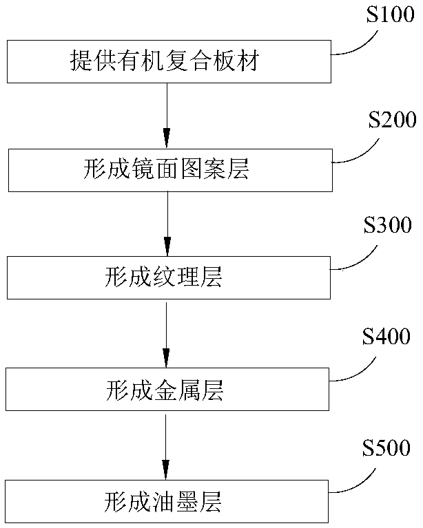
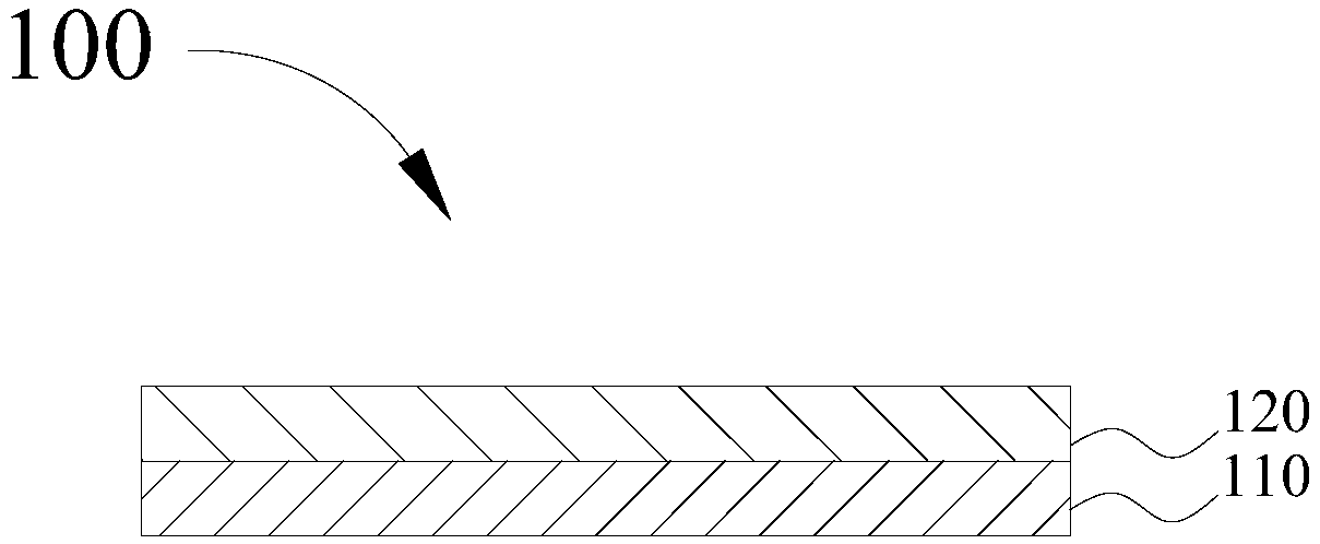
[0062] (1) Provide organic composite panels
[0063] The two-layer composite organic composite sheet formed by the PMMA sublayer and the PC sublayer, wherein the total thickness of the organic composite sheet is 0.5 mm, the thickness of the polycarbonate sublayer is 0.3 mm, and the thickness of the polymethylmethacrylate sublayer is 0.3 mm. The thickness is 0.2 mm.
[0064] (2) Form a mirror pattern layer
[0065] The mirror silver ink is printed on the polycarbonate sublayer by screen printing. After the mirror silver ink is partially dried, the printed mirror silver ink surface will have a mirror effect, and then baked at 60 degrees Celsius for 15 minutes , And finally form a mirror pattern layer.
[0066] (3) Form a texture layer
[0067] First make a transfer mold with bright surface texture; then print the UV transfer glue on the transfer mold by screen printing; then, put the organic composite board on the transfer mold, where the mirror pattern layer One side is in contact wit...
Embodiment 2
[0077] (1) Provide organic composite panels
[0078] The two-layer composite organic composite sheet formed by the PMMA sublayer and the PC sublayer, wherein the total thickness of the organic composite sheet is 0.5 mm, the thickness of the polycarbonate sublayer is 0.3 mm, and the thickness of the polymethylmethacrylate sublayer is 0.3 mm. The thickness is 0.2 mm.
[0079] (2) Form a mirror pattern layer
[0080] The method of forming the mirror pattern layer is the same as in the first embodiment.
[0081] (3) Form a texture layer
[0082] The method of forming the texture layer is the same as in the first embodiment. The thickness of the texture layer is 12 microns, and the light transmittance is 50%.
[0083] (4) Form metal layer
[0084] The method of forming the texture layer is the same as in the first embodiment. The thickness of the metal layer of indium is 25 nanometers, and the light transmittance of the metal layer may be 50%.
[0085] (5) Form the ink layer
[0086] The meth...
PUM
| Property | Measurement | Unit |
|---|---|---|
| Thickness | aaaaa | aaaaa |
| Thickness | aaaaa | aaaaa |
| Total thickness | aaaaa | aaaaa |
Abstract
Description
Claims
Application Information
 - R&D
- Intellectual Property
- Life Sciences
- Materials
- Tech Scout
- Unparalleled Data Quality
- Higher Quality Content
- 60% Fewer Hallucinations
Browse by: Latest US Patents, China's latest patents, Technical Efficacy Thesaurus, Application Domain, Technology Topic, Popular Technical Reports.
© 2025 PatSnap. All rights reserved.Legal|Privacy policy|Modern Slavery Act Transparency Statement|Sitemap|About US| Contact US: help@patsnap.com


