


Quick Research
Generate reliable direction feasibility study reports for your R&D in just a few steps.

Technical Q&A
Discover and master advanced knowledge NOW. Basics, ideas, possibilities, all at once.

Find Solutions
As an expert in R&D theories, this can generate solutions to your technical problems instantly.

Evaluate Feasibility
Analyze your overall solution with one click, know your potential R&D risks in advance.

Monitor Landscape
Get weekly tech updates, stay abreast of the latest tech innovations and key insights.
Trench step gate type IGBT chip
A trench gate and step technology, applied in electrical components, circuits, semiconductor devices, etc., can solve the problems of thick gate oxide layer, large heat loss, large chip, etc., to improve chip density, reduce switching loss, and enhance reflection. Effect of Latch Capability
- Summary
- Abstract
- Description
- Claims
- Application Information
AI Technical Summary
Problems solved by technology
Method used
Image

Examples
Embodiment 1
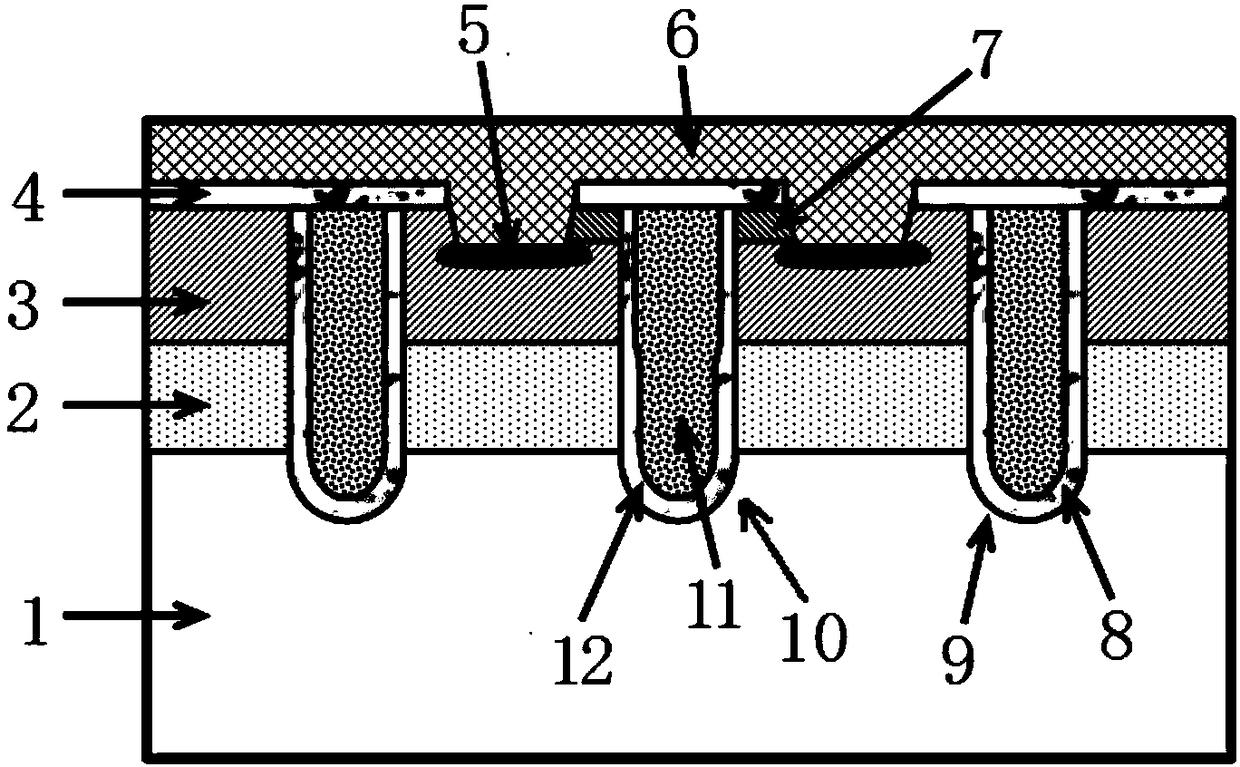
[0038] figure 2 A schematic cross-sectional view of a cell structure of a trench stepped gate IGBT chip provided in Embodiment 1 of the present invention, as shown in figure 2 As shown, the trench stepped gate IGBT chip of the present invention includes an N-type substrate 1 and a first trench gate and a second trench gate located in the surface of the substrate. The first trench gate structure is a real gate, and the second trench gate structure is a solid gate. The trench gate is a dummy gate, the real gate 10 and the dummy gate 9 are spaced apart, and the vertical gate oxide layer 12 of the real gate has a stepped shape, that is, the gate oxide layer 12 of the real gate is composed of different gate oxide thicknesses and is located above The gate oxide thickness of the gate oxide layer is smaller than the gate oxide thickness of the gate oxide layer located below, and the gate oxide layer 8 of the dummy gate 9 has a conventional gate oxide layer morphology.
[0039] The ...
Embodiment 2
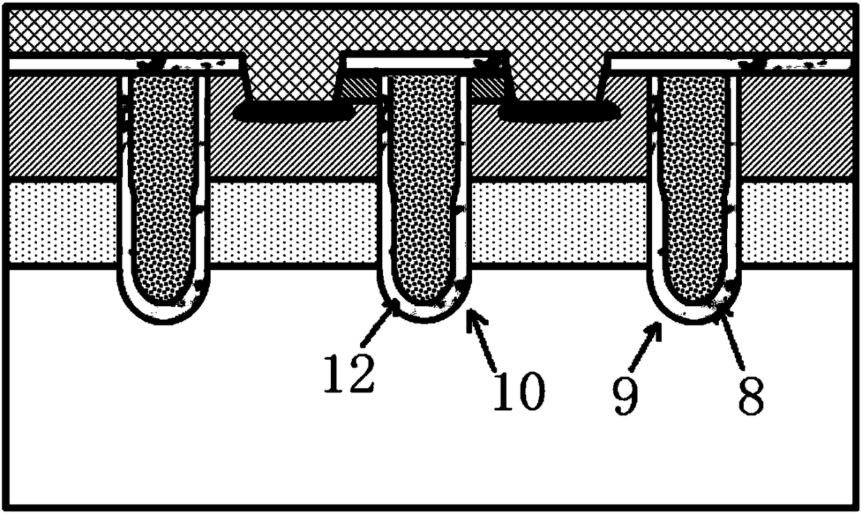
[0049] image 3 It is a schematic cross-sectional view of a cell structure of a trench step gate IGBT chip provided in Embodiment 2 of the present invention, as shown in image 3 As shown, the trench stepped gate IGBT chip of the present invention can be improved on the basis of the first embodiment, and includes an N-type substrate 1 and a first trench gate and a second trench gate located in the surface of the substrate. The first trench gate structure is a real gate, the second trench gate is a virtual gate 9, the real gate 10 and the virtual gate 9 are spaced apart, and the gate oxide layers of the real gate 10 and the virtual gate 9 are both stepped. The gate oxide layer 12 is composed of different gate oxide thicknesses, the gate oxide thickness of the gate oxide layer located above is smaller than the gate oxide thickness of the gate oxide layer located below, the gate oxide layer 8 of the virtual gate and the gate oxide of the real gate The gate oxide layers 12 are un...
Embodiment 3
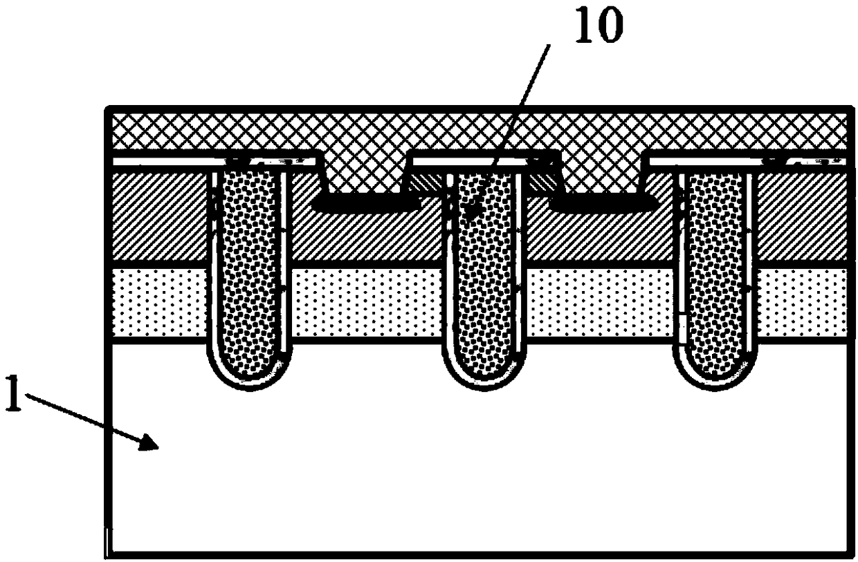
[0060] Figure 4 It is a schematic cross-sectional view of a cell structure of a trench step gate IGBT chip provided in Embodiment 1 of the present invention, as shown in Figure 4 As shown, the trench step gate IGBT chip of the third embodiment can be improved on the basis of the first embodiment or the second embodiment. The trench step gate IGBT chip of the present invention includes an N-type substrate 1 and a The real gate 10 in the surface has no virtual gate structure. The gate oxide layer of each real gate 10 has a stepped shape. The gate oxide layer 12 of the real gate is composed of different gate oxide thicknesses. The gate oxide thickness of the layer is less than the gate oxide thickness of the underlying gate oxide layer.
[0061] The gate oxide layer of the real gate consists of two different gate oxide thicknesses, the upper one is thinner than the traditional one, and the lower one is thicker. It can increase the chip density, reduce the power consumption an...
PUM
 Abstract
Description
Claims
Application Information
 - R&D Engineer
- R&D Manager
- IP Professional
- Industry Leading Data Capabilities
- Powerful AI technology
- Patent DNA Extraction
Browse by: Latest US Patents, China's latest patents, Technical Efficacy Thesaurus, Application Domain, Technology Topic, Popular Technical Reports.
© 2024 PatSnap. All rights reserved.Legal|Privacy policy|Modern Slavery Act Transparency Statement|Sitemap|About US| Contact US: help@patsnap.com