


Quick Research
Generate reliable direction feasibility study reports for your R&D in just a few steps.

Technical Q&A
Discover and master advanced knowledge NOW. Basics, ideas, possibilities, all at once.

Find Solutions
As an expert in R&D theories, this can generate solutions to your technical problems instantly.

Evaluate Feasibility
Analyze your overall solution with one click, know your potential R&D risks in advance.

Monitor Landscape
Get weekly tech updates, stay abreast of the latest tech innovations and key insights.
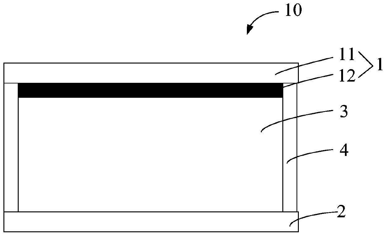
Photodetector and its preparation method
A photodetector and ultraviolet light technology, which is applied in photosensitive equipment, semiconductor devices, nanotechnology for materials and surface science, etc., can solve the problems of poor stability of two-dimensional nanomaterials, poor performance of photodetectors, and short detection wavelengths and other problems, to achieve the effect of simple and easy operation, good photoelectric detection performance and long service life
- Summary
- Abstract
- Description
- Claims
- Application Information
AI Technical Summary
Problems solved by technology
Method used
Image

Examples
preparation example Construction
[0048] The second aspect of the present invention provides a method for preparing a photodetector, comprising the following steps:
[0049] S01, providing a tellurium raw material, and exfoliating the tellurium raw material by a liquid phase exfoliation method to obtain two-dimensional tellurium nanosheets;
[0050] S02, dispersing the two-dimensional tellurium nanosheets in an organic solvent to form a two-dimensional tellurium nanosheet dispersion, uniformly coating the two-dimensional tellurium nanosheet dispersion on a conductive substrate, and drying to obtain a working electrode;
[0051] S03, providing a counter electrode, injecting an electrolyte solution between the working electrode and the counter electrode, and obtaining a photodetector after packaging.
[0052] In the embodiment of the present invention, in step S01, the tellurium raw material is a two-dimensional non-layered metal tellurium element, such as tellurium powder, or a tellurium block, and there is no ...
Embodiment 1
[0077] A method for preparing two-dimensional tellurium nanosheets, comprising the following steps:
[0078] (1) Add 500mg of tellurium powder into 100ml of isopropanol. Then select the probe ultrasound 240W, ultrasound 10h. The ultrasonic on / off time was selected as 2 / 4s, and the ultrasonic was performed in an ice bath environment. After the probe is sonicated, the water bath is then used for sonication. The ultrasonic power of the water bath is 360W. Ultrasonic time is 8h. The temperature of the water bath was maintained at 10°C;
[0079] (2) After ultrasonication, centrifugation is used to obtain the required two-dimensional tellurium nanosheets. Firstly, a centrifugal force of 2000g is used for 30min. The supernatant was taken, and then the supernatant was centrifuged at 12000g for 30 minutes to obtain a precipitate, which was dried in vacuum to obtain two-dimensional tellurium nanosheets.
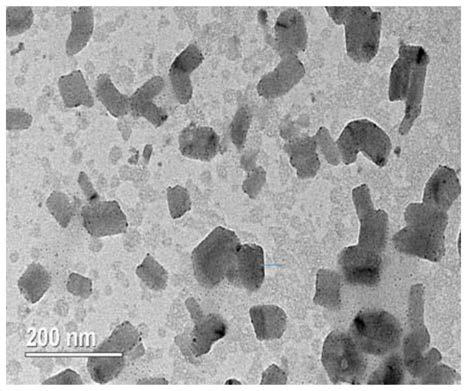
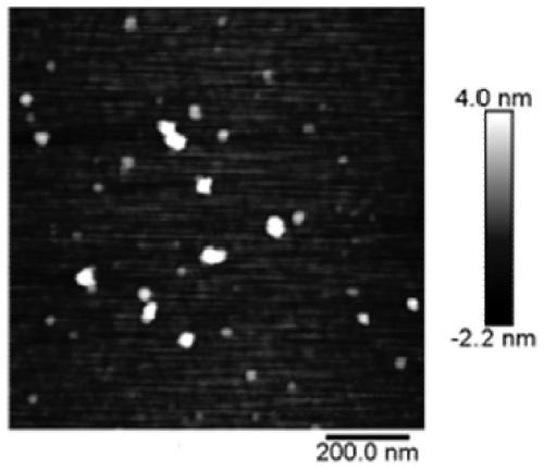
[0080] Such as figure 2 Shown is the electron microscope topography of tw...
Embodiment 2
[0084] A method for preparing two-dimensional tellurium nanosheets, comprising the following steps:
[0085] (1) Add 500mg of tellurium powder into 100ml of isopropanol. Then select the probe ultrasound 200W, ultrasound 15h. The ultrasonic on / off time was selected as 2 / 4s, and the ultrasonic was performed in an ice bath environment. After the probe is sonicated, the water bath is then used for sonication. The ultrasonic power of the water bath is 300W. Ultrasonic time is 10h. The temperature of the water bath was maintained at 15°C;
[0086](2) After ultrasonication, centrifugation is used to obtain the required two-dimensional tellurium nanosheets. Firstly, the centrifugal force of 1800g is adopted, and the centrifugation is performed for 35min. The supernatant was taken, and then the supernatant was centrifuged at 15000 g for 25 minutes to obtain a precipitate, which was vacuum-dried to obtain two-dimensional tellurium nanosheets.
PUM
| Property | Measurement | Unit |
|---|---|---|
| thickness | aaaaa | aaaaa |
| size | aaaaa | aaaaa |
| thickness | aaaaa | aaaaa |
Abstract
Description
Claims
Application Information
 - R&D Engineer
- R&D Manager
- IP Professional
- Industry Leading Data Capabilities
- Powerful AI technology
- Patent DNA Extraction
Browse by: Latest US Patents, China's latest patents, Technical Efficacy Thesaurus, Application Domain, Technology Topic, Popular Technical Reports.
© 2024 PatSnap. All rights reserved.Legal|Privacy policy|Modern Slavery Act Transparency Statement|Sitemap|About US| Contact US: help@patsnap.com