CsPbX3 nano-crystal doped boron-containing glass and preparation method thereof
A technology of nanocrystalline and boron glass, which is applied in the field of CsPbX3 nanocrystalline doped boron-containing glass and its preparation, can solve the problems of poor optical quality of glass and difficulty in meeting application requirements, and achieve the promotion of clarification and homogenization, and the nanocrystalline size can be adjusted control, the effect of excellent optical performance
- Summary
- Abstract
- Description
- Claims
- Application Information
AI Technical Summary
Problems solved by technology
Method used
Image
Examples
Embodiment 1
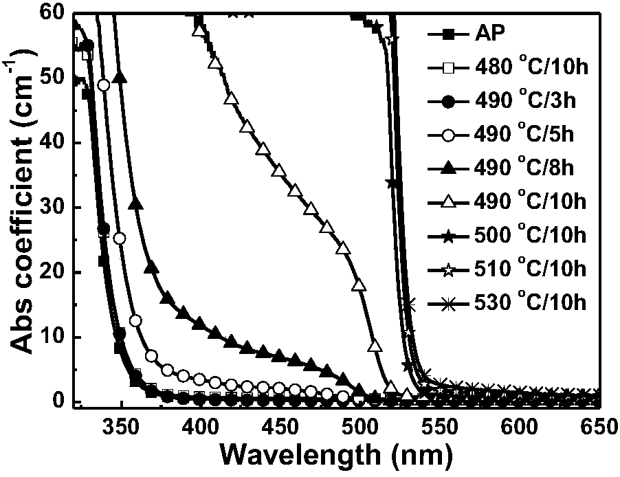
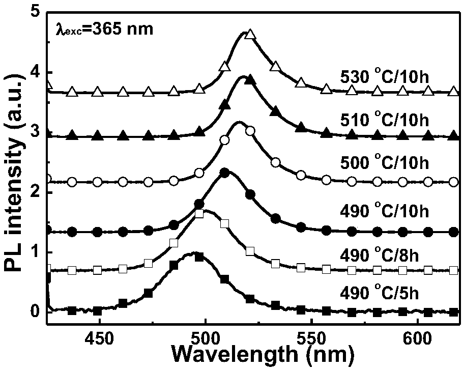
[0046] Weigh raw materials according to the following atomic mole percentages, Si: 4.71%, B: 27.75%, O: 56.94%, Cs: 1.05%, Pb: 1.31%, Br: 2.09%, Ca: 3.14%, Na: 2.09%, Zn : 0.92%. After mixing evenly, melt at 1100-1300°C for 20-60 minutes, then cool to shape, and anneal at about 350°C to eliminate residual stress to obtain transparent glass (hereinafter referred to as original glass, represented by AP). Cut it into a specific size, treat it at 480-530°C for 3-10 hours, and cool it to room temperature with the furnace to obtain CsPbBr 3 The nanocrystal-doped transparent glass is polished and tested. figure 1 and figure 2 It is the original glass and its absorption spectrum under different heat treatment temperature and time, AP represents the original glass sample without heat treatment, 480℃ / 10h, etc. represent the heat treatment temperature and time conditions, figure 2 It is the fluorescence spectrogram of the sample in this example under 365nm laser excitation. It can ...
Embodiment 2
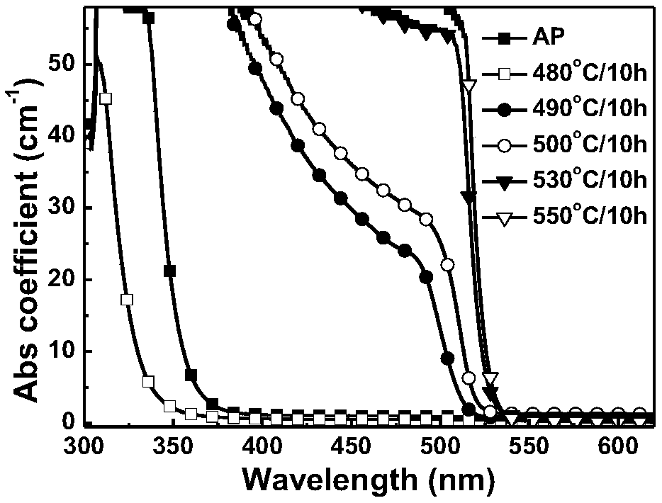
[0048] The raw materials were weighed according to the following atomic mole percentages, B: 33.90%, O: 56.17%, Ca: 3.15%, Cs: 1.45%, Pb: 1.45%, Br: 1.94%, Na: 1.94%. After mixing evenly, melt at 1100-1300°C for 20-60 minutes, then cool to shape, and anneal at about 350°C to eliminate residual stress to obtain transparent glass. Cut it into a specific size, treat it at 480-550°C for 10 hours, and cool it to room temperature with the furnace to obtain CsPbBr 3 The nanocrystal-doped transparent glass is polished and tested. Absorption spectra and fluorescence spectra of samples under different heat treatment temperatures and times, as shown in image 3 and Figure 4 As shown, the adjustable range of fluorescence peak wavelength is 503-518nm, and the quantum efficiency of the glass sample treated at 500°C for 10h is 21.4%.
Embodiment 3
[0050] Weigh raw materials according to the following atomic mole percentages, Si: 5.33%, B: 26.67%, O: 54.95%, Cs: 2.66%, Pb: 0.8%, I: 3.73%, Ca: 0%, Na: 3.73%, Zn : 2.13%, mixed evenly and melted at 1100-1300°C for 20-60 minutes, then cooled and formed, and annealed at about 350°C to eliminate residual stress to obtain transparent glass. Cut it into a specific size, treat it at 440-500°C for 3-10 hours, and cool it to room temperature with the furnace to obtain CsPbI 3 The nanocrystal-doped transparent glass is polished and tested. Absorption spectra and fluorescence spectra of samples under different heat treatment temperatures and times, as shown in Figure 5 and Figure 6 As shown, the adjustable range of fluorescence peak wavelength is 644-696nm, and the quantum efficiency of the glass sample treated at 480°C for 10h is 20.8%.
PUM
 Abstract
Description
Claims
Application Information
 - R&D Engineer
- R&D Manager
- IP Professional
- Industry Leading Data Capabilities
- Powerful AI technology
- Patent DNA Extraction
Browse by: Latest US Patents, China's latest patents, Technical Efficacy Thesaurus, Application Domain, Technology Topic, Popular Technical Reports.
© 2024 PatSnap. All rights reserved.Legal|Privacy policy|Modern Slavery Act Transparency Statement|Sitemap|About US| Contact US: help@patsnap.com


