
Method for preparing metal sulfur group compound semiconductor ultrafine ultra-long nano-wires, and nano-wires prepared through method

A compound and semiconductor technology, used in metal selenide/telluride, selenium/tellurium compounds, chemical instruments and methods, etc., to achieve good crystallinity, wide application value, and remarkable quantum confinement effect.

Active Publication Date: 2018-08-14
BEIJING NORMAL UNIVERSITY
View PDF2 Cites 0 Cited by
  • Summary
  • Abstract
  • Description
  • Claims
  • Application Information

AI Technical Summary

Problems solved by technology

However, it should be pointed out that the solvothermal environment can easily promote the ripening of nanocrystals to form thicker nanowires or particles.
At present, there is no report on the synthesis of different types of ultra-fine and ultra-long nanowires by solvothermal method

Method used


Image

  • Method for preparing metal sulfur group compound semiconductor ultrafine ultra-long nano-wires, and nano-wires prepared through method
  • Method for preparing metal sulfur group compound semiconductor ultrafine ultra-long nano-wires, and nano-wires prepared through method
  • Method for preparing metal sulfur group compound semiconductor ultrafine ultra-long nano-wires, and nano-wires prepared through method

Examples


Embodiment 1

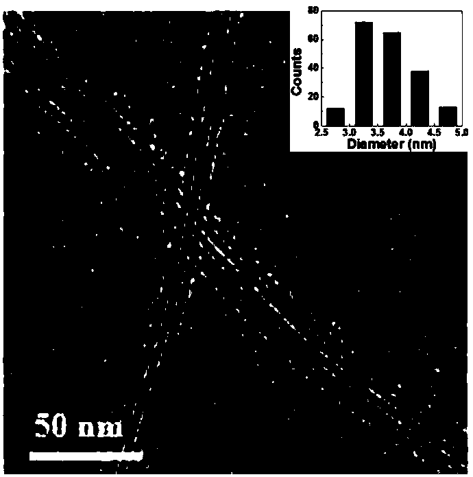
[0041] Embodiment 1, the preparation of ZnTe nanowires with an average diameter of 3.5nm

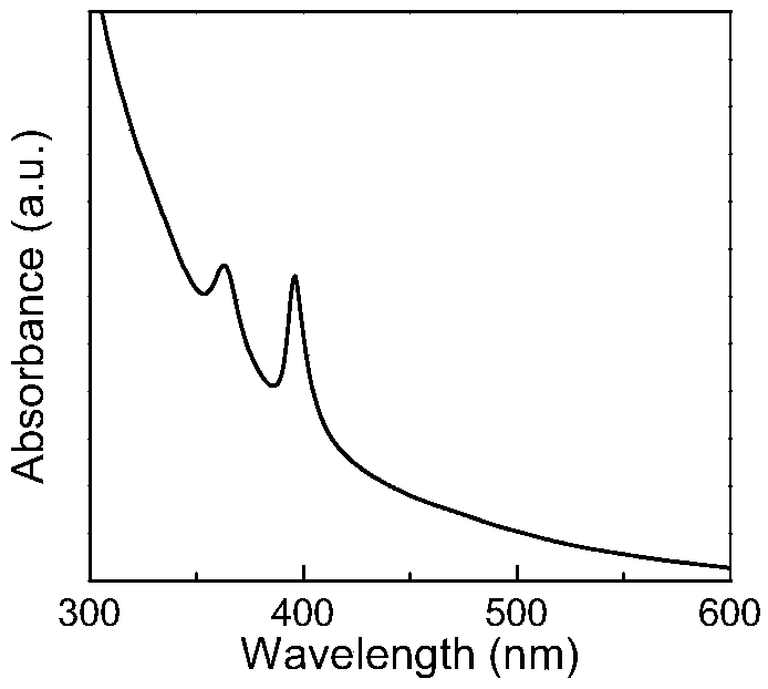
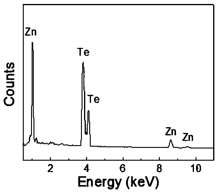
[0042] (1) Preparation of zinc precursor: 0.2~1.0mmol Zn(NO 3 ) 2 or ZnCl 2 Mix it with 6.0-15mL of octylamine or oleylamine or tri-n-octylphosphine oxide and add it to the container. Under the protection of inert gas, stir and heat until clear, and then the solution drops to room temperature, that is, the zinc precursor solution.

[0043] Among them, Zn(NO 3 ) 2 or ZnCl 2 The amount is 0.2-1.0 mmol, the amount of octylamine or oleylamine or tri-n-octylphosphine oxide is 6.0-15 mL, and the molar ratio of the metal precursor to the organic ligand is 1:20-50.

[0044] (2) Preparation of tellurium precursor: add 0.1-1.0 mmol tellurium powder or tellurium dioxide or sodium tellurite and 1.0-2.0 mL tri-n-octylphosphine or tri-n-butylphosphine into a container filled with argon or nitrogen , the mixture was stirred and heated until clear, and cooled to room temperature, that is, the prec...

Embodiment 2

[0047] Embodiment 2, the average diameter is the preparation of the CdTe nanowire of 4.8nm

[0048] The choice of cadmium removal precursor is 0.2~1.0mmol Cd(Ac) 2 or Cd(NO 3 ) 2 Except, other synthesis steps are the same as in Example 1. Such as Figure 4 Shown is the absorption spectrum of the CdTe nanowires prepared in Example 5. from Image 6 It can be known from the composition analysis that its constituent elements are Cd and Te. Figure 7 with Figure 8 It is the transmission electron microscope picture of CdTe nanowire, as can be seen from the figure that the CdTe nanowire prepared by the method of the present invention is an ultrafine nanowire, the average length of the nanowire is about 7 μm, and the average diameter is 4.8nm, and its aspect ratio About 1400:1.

Embodiment 3

[0049] Embodiment 3, the preparation of the ZnSe nano wire that average diameter is 3.4nm

[0050] The choice of selenium removal precursor is 0.1 ~ 1mmol selenium powder or selenourea or selenium dioxide and 1 ~ 2mL C 8 ~C 18 Except that alkylamine is used as an activator, other synthesis steps are the same as in Example 1. Such as Figure 9 Shown is the absorption spectrum of the ZnSe nanowires prepared in Example 3. from Figure 10 It can be known from the composition analysis that its constituent elements are Zn and Se. Figure 11 with Figure 12 It is the transmission electron microscope figure of ZnSe nanowire, as can be seen from the figure that the ZnSe nanowire prepared by the inventive method is an ultrafine nanowire, and the average length of the nanowire is about 5 μm, and the average diameter is 3.4nm, and its aspect ratio About 1400:1.


PUM

PropertyMeasurementUnit
diameteraaaaaaaaaa
lengthaaaaaaaaaa
diameteraaaaaaaaaa

Abstract

The invention relates to the field of synthesis of nanometer materials, particularly to a method for preparing metal sulfur group compound semiconductor ultrafine ultra-long nano-wires, and the nano-wires prepared through the method. The method comprises: preparing a metal precursor and a non-metal precursor; and placing the metal precursor solution and the non-metal precursor solution in a high pressure kettle, and carrying out a solvothermal reaction under optimized reaction conditions to obtain the metal sulfur group compound semiconductor ultrafine ultra-long nano-wires. According to the present invention, the synthesis method has universality, and can synthesize a plurality of different metal sulfur group compound semiconductor ultrafine ultra-long nano-wires; and the prepared metal sulfur group compound semiconductor ultrafine ultra-long nano-wires have characteristics of uniform morphology, good crystallinity and significant quantum confinement effect, has the wire diameter of 5nm and the aspect ratio of more than 300, and are the ideal constructing unit for nanometer optical devices.

Description

technical field [0001] The invention relates to the field of nanomaterial synthesis, in particular to a method for preparing metal chalcogenide semiconductor ultra-fine and ultra-long nanowires and the prepared nanowires. Background technique [0002] Ultra-thin and ultra-long semiconductor nanowires refer to semiconductor nanowires whose wire diameter is less than 5nm (or even 3nm) and obviously smaller than its Bohr excitonic radius, and whose aspect ratio is greater than 300 (or even 1000). Compared with conventional semiconductor nanowires whose diameter is usually greater than 10nm, ultra-thin and ultra-long semiconductor nanowires not only have stronger quantum confinement effect, more significant surface effect and More novel physical and chemical properties, but also an ideal building block for a new generation of nano-optical / electronic devices, photoelectric conversion devices, light-emitting display devices, detection and sensing devices. Therefore, the synthesis...

Claims


Application Information

Patent Timeline
Patent Type & Authority Applications(China)
IPC IPC(8): C01B19/00C01G9/08
CPCC01B19/007C01G9/08C01P2004/04C01P2004/16
Inventor 李运超李冬邢观洁唐世霖
Owner BEIJING NORMAL UNIVERSITY
Learn More