A kind of preparation method of semiconductor interconnection structure

A technology of semiconductor and interconnection structure, applied in semiconductor/solid-state device manufacturing, electrical components, circuits, etc., can solve the impact of semiconductor device stability and reliability, interlayer dielectric layer damage or pollution, interlayer dielectric layer dielectric constant Drift and other issues, to achieve the effect of shortening the etching time

Active Publication Date: 2020-09-11
XINYI XIYI ADVANCED MATERIALS RES INST OF IND TECH CO LTD
View PDF4 Cites 0 Cited by
  • Summary
  • Abstract
  • Description
  • Claims
  • Application Information

AI Technical Summary

Problems solved by technology

[0004] However, the use of low-K or ultra-low-K insulating dielectric materials poses new requirements for semiconductor manufacturing processes. On the one hand, in order to obtain low-K materials or ultra-low-K materials and reduce the K value of materials, the materials usually used are porous materials. However, the mechanical strength of porous materials is relatively low, which leads to easy damage to the insulating dielectric layer during the process of etching through holes or trenches. On the other hand, the porous insulating dielectric layer is easily infiltrated by external materials, causing pollution , reducing the reliability of the material
[0005] At the same time, when forming the through hole or trench structure of the interconnection structure, photolithography technology and etching steps need to be used multiple times. In the photolithography step and etching step, the mask layer needs to be removed after etching. When removing the mask layer in the prior art, dry or wet etching steps are used, so that although the subsequent unnecessary mask structure can be removed more accurately, it will inevitably cause damage to the underlying interlayer dielectric layer Or pollution, which will cause the dielectric constant of the interlayer dielectric layer to drift, resulting in a change in the capacitance value of the interlayer dielectric layer; and there are other interconnections under the via holes or trenches formed by the interlayer dielectric layer When etching, it is easy to cause damage to the underlying interconnection structure, which will have a great impact on the stability and reliability of semiconductor devices

Method used


Image

  • A kind of preparation method of semiconductor interconnection structure
  • A kind of preparation method of semiconductor interconnection structure
  • A kind of preparation method of semiconductor interconnection structure

Examples


Embodiment Construction

[0027] In the following description, the method for preparing the semiconductor interconnection structure proposed by the present invention will be further described in detail with reference to the accompanying drawings and examples, in order to provide a more thorough understanding of the present invention through specific details. It should be noted that all the drawings are in a very simplified form and use imprecise scales, and are only used to facilitate and clearly assist the purpose of illustrating the embodiments of the present invention. In the embodiments, in order to avoid confusion with the present invention, some technical features known in the art are not described.

[0028] Please refer to the attached figure 1 The schematic diagram of the preparation process of the present invention shown, the preparation method includes the following process steps:

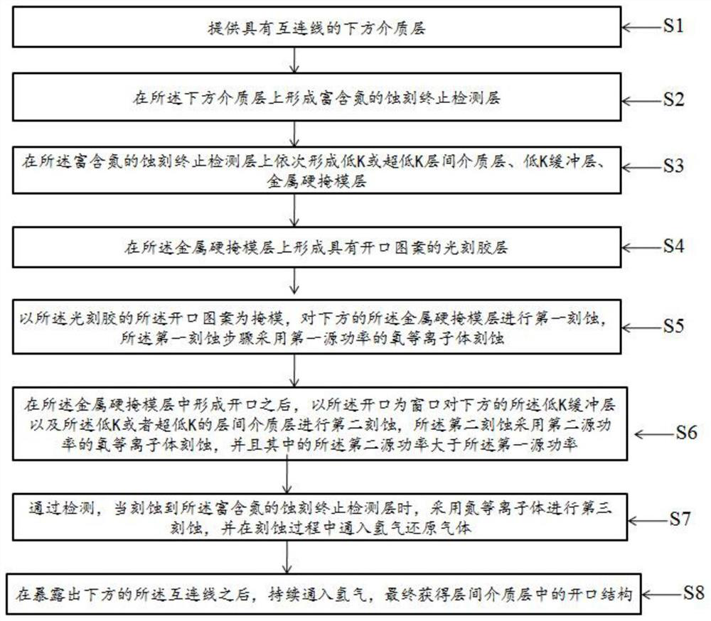
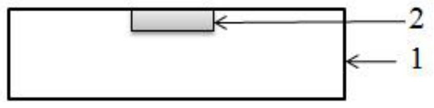
[0029] Step S1: providing a lower dielectric layer with interconnection lines;

[0030] Step S2: forming a ni...


PUM

PropertyMeasurementUnit
thicknessaaaaaaaaaa
thicknessaaaaaaaaaa
thicknessaaaaaaaaaa

Abstract

The invention relates to a preparation method of a semiconductor interconnection structure. The preparation method includes: providing a lower medium layer with interconnection lines; forming a nitrogen-rich etch stop detection layer, an interlaminar dielectric layer, a low-K buffer layer and a metal hard mask layer in sequence; forming a lithography glue layer with an opening pattern on the metalhard mask layer, and subjecting the lower metal hard mask layer to first etching by taking the opening patter of lithography glue as a mask; after the opening is formed in the metal hard mask layer,subjecting the lower structure to second etching, wherein the second etching adopts oxygen plasma etching of second source power, and the second source power is greater than first source power; when the nitrogen-rich etch stop detection layer is etched, adopting a nitrogen plasma for third etching and inletting hydrogen reduction gas during etching; after the lower interconnection lines are exposed, continuously inletting nitrogen till the opening structure in the interlaminar dielectric layer is obtained.

Description

technical field [0001] The invention relates to a method for preparing a semiconductor interconnection structure, in particular to a method for preparing an interconnection structure with a low-K or ultra-low-K interlayer dielectric layer. Background technique [0002] The rapid development of semiconductor integrated circuit technology constantly puts forward new requirements for the development of interconnection technology. At present, in the back-end process of semiconductor manufacturing, in order to connect the integrated circuits composed of various components, metal materials with relatively high conductivity are usually used, but as the size of semiconductor devices continues to shrink, the interconnection structure becomes narrower and narrower. , resulting in higher and higher interconnect resistances. With the help of copper's excellent electrical conductivity, copper interconnection technology has been widely used in the technology of 90nm and 65nm technology n...

Claims


Application Information

Patent Timeline
Patent Type & Authority Patents(China)
IPC IPC(8): H01L21/768H01L21/311
CPCH01L21/31144H01L21/76802
Inventor 赵红英
Owner XINYI XIYI ADVANCED MATERIALS RES INST OF IND TECH CO LTD
Why Eureka
Try Eureka