High-reliability inorganic all-solid-state electrochromic film device and preparing method thereof

An electrochromic, thin-film device technology, applied in instruments, nonlinear optics, optics, etc., can solve the problems of low yield of film forming and high production cost, achieve precise control of light passing rate, prolong life, and improve response time. Effect

Inactive Publication Date: 2018-07-13
安徽鑫昊等离子显示器件有限公司
View PDF7 Cites 6 Cited by
  • Summary
  • Abstract
  • Description
  • Claims
  • Application Information

AI Technical Summary

Problems solved by technology

The all-solid-state thin-film electrochromic glass is composed of solid materials, which increases the stability of the product, but the yield of thin-film molding is low and the production cost is high

Method used


Image

  • High-reliability inorganic all-solid-state electrochromic film device and preparing method thereof
  • High-reliability inorganic all-solid-state electrochromic film device and preparing method thereof
  • High-reliability inorganic all-solid-state electrochromic film device and preparing method thereof

Examples


preparation example Construction

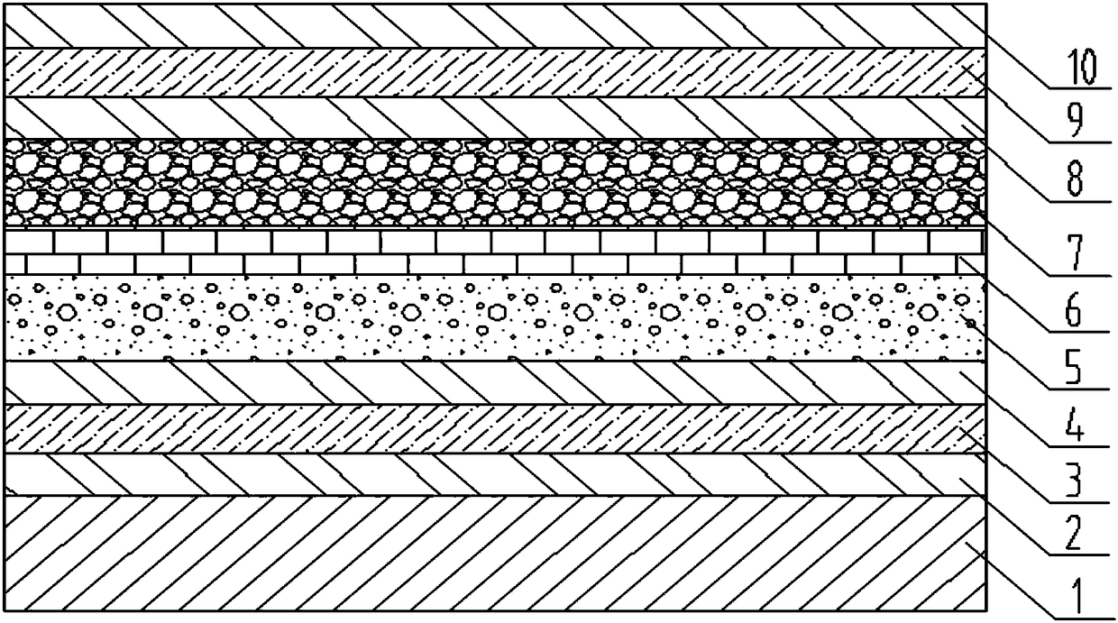
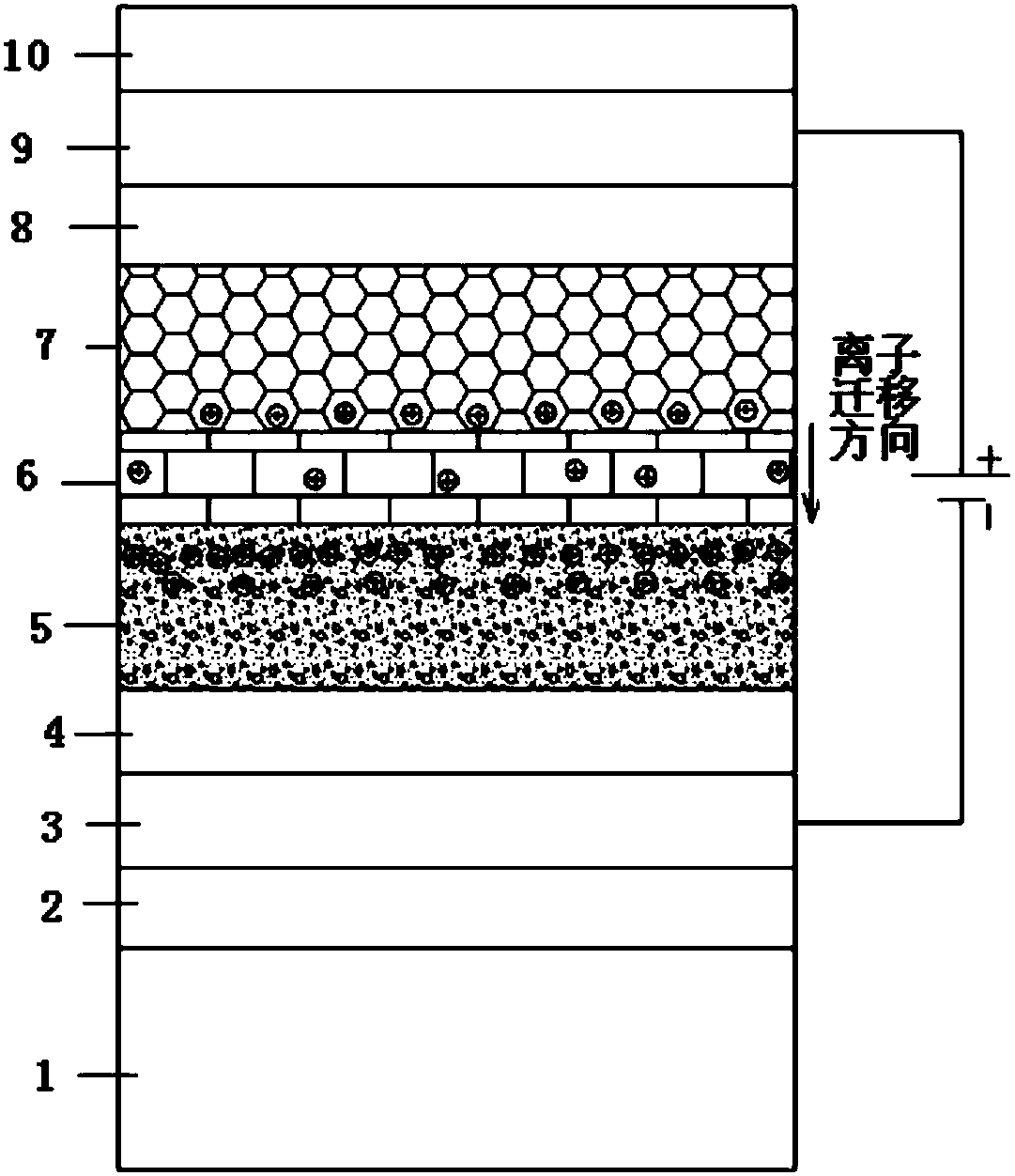
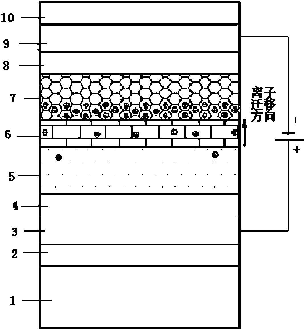
[0056] An embodiment of the present invention provides a method for preparing an inorganic all-solid-state electrochromic thin film device, comprising the following steps: forming a first protective layer, a first transparent conductor layer, and a second protective layer on a substrate in sequence by vapor deposition. layer, an inorganic color-changing layer, an inorganic ion-conducting layer, an inorganic ion storage layer, a third protective layer, a second transparent conductor layer and a fourth protective layer to obtain an inorganic all-solid-state electrochromic thin film device.

[0057] In the embodiment of the present invention, the substrate can be washed, dried, and then put into a coating system to form the above-mentioned film layers in sequence. The contents of the substrate and each layer are as described above, and will not be repeated here.

[0058]Physical vapor deposition (Physical Vapor Deposition, PVD) technology refers to the use of physical methods und...

Embodiment 1

[0065] The device structure of the film-layer combination in this embodiment is as follows: using ultra-clear glass with a thickness of 1.8 mm as the substrate, sequentially formed: bottom protective layer: silicon dioxide; bottom transparent conductor layer: indium tin oxide; protective layer: silicon dioxide; color-changing layer : tungsten oxide layer; ion conductor layer: lithium tungsten oxide layer; ion storage layer: lithium-doped tungsten nickel oxide layer; protective layer, silicon oxide; top transparent electrode layer: indium tin oxide; top protective layer, silicon dioxide.

[0066] The specific manufacturing process is as follows:

[0067] (1) The glass substrate is cleaned and dried, and enters the coating system.

[0068] (2) Intermediate frequency reactive sputtering rotating silicon target to prepare silicon dioxide; set power AC 30KW, atmosphere: argon and oxygen mixed, air pressure 3×10 -4 mbar, film thickness 20nm.

[0069] (3) Magnetron sputtering rotat...

Embodiment 2

[0079] The device structure of the film layer combination of this embodiment is the same as that of Embodiment 1;

[0080] The difference in the specific manufacturing process is: using a rotating lithium tungsten oxide target to directly form a lithium tungsten oxide layer; radio frequency 13.56MHz, the atmosphere is mixed with argon and oxygen, and the mixed volume ratio Ar 2 :O 2 =2:3, air pressure 8×10 -4 mbar, forming a lithium tungsten oxide layer with a thickness of 200nm.


PUM

PropertyMeasurementUnit
thicknessaaaaaaaaaa
thicknessaaaaaaaaaa
thicknessaaaaaaaaaa

Abstract

The invention provides a high-reliability inorganic all-solid-state electrochromic film device and a preparing method thereof. The device comprises a substrate, and a first protection layer, a first transparent conductor layer, a second protection layer, an inorganic discoloring layer, an inorganic ionic conduction layer, an inorganic ion storage layer, a third protection layer, a third transparent conductor layer and a fourth protection layer which are arranged on the substrate in sequence. The film combination is of an all-solid-state structure, all film layers are in inorganic solid states,the activity of film materials cannot degrade or reduce over time, or there is no mutual corrosion problem among the materials. In the high-reliability inorganic all-solid-state electrochromic film device, the protection layers arranged mainly to avoid short circuit inside the transparent conductor layers and discoloration and failure. Therefore, the performance of all the film layers is strengthened, the light pass rate can be controlled precisely, the response time is prolonged, the good-product rate of shaped films is increased, the service life of the electrochromic device is prolonged, and the cost is reduced.

Description

technical field [0001] The invention relates to the field of electrochemical devices with electrically controllable reversible optics and / or energy transmission characteristics, in particular to an inorganic all-solid-state electrochromic thin film device and a preparation method thereof, which have high yield and reliability. Background technique [0002] With the rapid growth of the world economy, great achievements have been made at the cost of resources and the environment, and the contradiction between economic development and resources and environment has become increasingly acute. The demand for energy is tense, and global warming caused by greenhouse gas emissions is becoming more and more obvious. Therefore, it is particularly important to develop new energy-saving materials and strengthen energy-saving and emission-reduction work. For traditional glass, it can only fix and change the transmittance of light, so electrochromic glass came into being, which belongs to ...

Claims


Application Information

Patent Timeline
Patent Type & Authority Applications(China)
IPC IPC(8): G02F1/153C03C17/34
CPCC03C17/3417C03C2217/213C03C2217/219C03C2217/23C03C2217/231C03C2218/154C03C2218/155C03C2218/156G02F1/1533G02F2001/1536
Inventor 袁浩王海强章婷吴琼
Owner 安徽鑫昊等离子显示器件有限公司
Why Eureka
Try Eureka