Nano multilayered silicon nitride ceramic coating and preparation method and application thereof
A silicon nitride ceramic and nano-multilayer technology is applied in the field of silicon nitride coating and nano-multilayer ultra-thick silicon nitride ceramic coating, which can solve the overall performance decline of micro-crack coating and limit the service safety of the coating. and stability, difficult to prepare large samples, etc., to achieve the effect of no macroscopic defects, improved service safety, and small size restrictions
- Summary
- Abstract
- Description
- Claims
- Application Information
AI Technical Summary
Problems solved by technology
Method used
Image

Examples
preparation example Construction
[0035] One aspect of the embodiments of the present invention provides a method for preparing a nano-multilayer silicon nitride ceramic coating, which includes:
[0036] Provide the substrate;
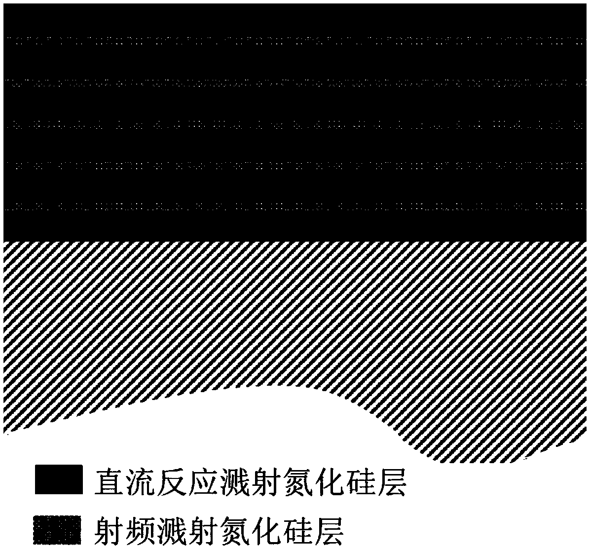
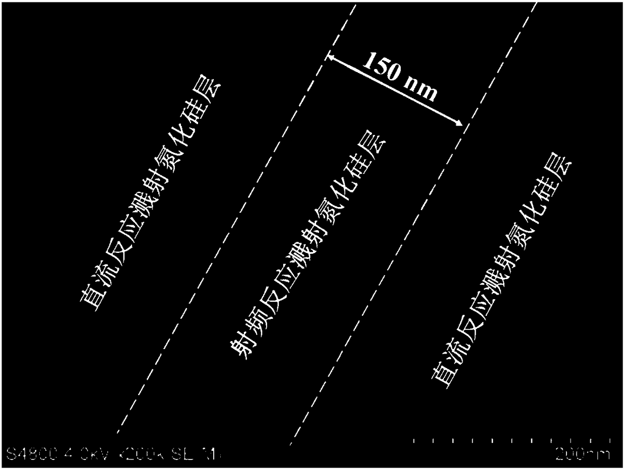
[0037] Using single crystal silicon target and / or silicon nitride target as cathode, and using inert gas and nitrogen as working gas, using DC reactive sputtering technology and radio frequency sputtering technology to deposit and form the nanometer multilayer nitrogen on the substrate A silicon nitride ceramic coating, the nanometer multi-layer silicon nitride ceramic coating comprises alternately stacked DC reactive sputtering silicon nitride layers and radio frequency sputtering silicon nitride layers.
[0038] In some embodiments, the preparation method specifically includes:
[0039] (1) Provide substrate;
[0040] (2) cleaning the substrate by plasma sputtering;
[0041] (3) Using single crystal silicon target and / or silicon nitride target as cathode, and using inert gas and n...
Embodiment 1
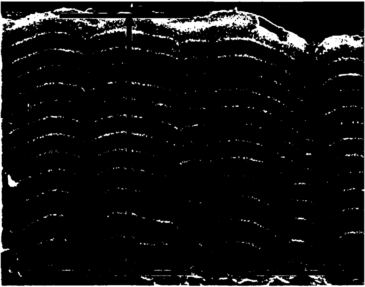
[0077] Example 1 The nano-multilayer ultra-thick silicon nitride ceramic coating is a dense silicon nitride coating with a thickness of 24.3 μm deposited on a porous ceramic substrate. The coating has a hardness of 13.9 GPa and a plastic deformation rate of 65%.
[0078] The preparation process of the nanometer multi-layer ultra-thick silicon nitride coating is carried out according to the following steps:
[0079] (1) Plasma sputtering to clean the base material. First, use ethanol and acetone to ultrasonically clean the ceramic substrate. After drying, put it into the vacuum chamber of the magnetron sputtering equipment for argon plasma sputtering cleaning. The specific process is: argon gas flow rate 120sccm , bias voltage -500V, processing time 30min;
[0080] (2) DC reactive sputtering deposition of DC reactive sputtering silicon nitride coating (referred to as DC silicon nitride layer), the single crystal silicon target is selected as the cathode, and the vacuum chamber ...
Embodiment 2
[0090] Example 2 The nanometer multilayer ultra-thick silicon nitride ceramic coating (also known as silicon nitride-based sealing coating) is a dense silicon nitride coating with a thickness of 26.3 μm deposited on a porous ceramic substrate. The hardness is 11.6GPa, and the plastic deformation rate is 68%.
[0091] The preparation process of the nanometer multi-layer ultra-thick silicon nitride coating is carried out according to the following steps:
[0092] (1) Plasma sputtering to clean the base material. First, use ethanol and acetone to ultrasonically clean the ceramic substrate. After drying, put it into the vacuum chamber of the magnetron sputtering equipment for argon plasma sputtering cleaning. The specific process is: argon gas flow rate 120sccm , bias voltage -500V, processing time 30min;
[0093] (2) DC reactive sputtering to deposit silicon nitride coating, choose single crystal silicon target as cathode, vacuum chamber pressure is 8.0*10 - 1 Pa, the power of...
PUM
| Property | Measurement | Unit |
|---|---|---|
| thickness | aaaaa | aaaaa |
| thickness | aaaaa | aaaaa |
| thickness | aaaaa | aaaaa |
Abstract
Description
Claims
Application Information
 - R&D
- Intellectual Property
- Life Sciences
- Materials
- Tech Scout
- Unparalleled Data Quality
- Higher Quality Content
- 60% Fewer Hallucinations
Browse by: Latest US Patents, China's latest patents, Technical Efficacy Thesaurus, Application Domain, Technology Topic, Popular Technical Reports.
© 2025 PatSnap. All rights reserved.Legal|Privacy policy|Modern Slavery Act Transparency Statement|Sitemap|About US| Contact US: help@patsnap.com