
Infrared optical window with three-step anti-reflection structure and preparation method thereof

A technology of infrared optical window and reflective structure, which is applied in the field of infrared optical window, can solve the problems of low transmittance of single-step anti-reflection structure, excessive deviation of step height influence, narrow bandwidth, etc., so as to reduce the difficulty of processing and improve the process Tolerance, the effect of enhancing stability

Pending Publication Date: 2018-07-06
UNIV OF ELECTRONIC SCI & TECH OF CHINA
View PDF7 Cites 7 Cited by
  • Summary
  • Abstract
  • Description
  • Claims
  • Application Information

AI Technical Summary

Problems solved by technology

[0005] The purpose of the present invention is to solve the problem that the transmittance of the current single-step anti-reflection structure is low, the bandwidth is too narrow, the diffraction effect of the single-step structure during exposure in the photolithography process has too much influence on the deviation of the graphic parameters, and the The slight change of process parameters has too much influence on the deviation of the obtained step height, and an infrared optical window with a three-step anti-reflection structure and its preparation method are provided

Method used


Image

  • Infrared optical window with three-step anti-reflection structure and preparation method thereof
  • Infrared optical window with three-step anti-reflection structure and preparation method thereof
  • Infrared optical window with three-step anti-reflection structure and preparation method thereof

Examples


Embodiment Construction

[0067] In order to make the object, technical solution and advantages of the present invention clearer, the present invention will be further described in detail below in conjunction with the accompanying drawings and embodiments. It should be understood that the specific embodiments described here are only used to explain the present invention, not to limit the present invention.

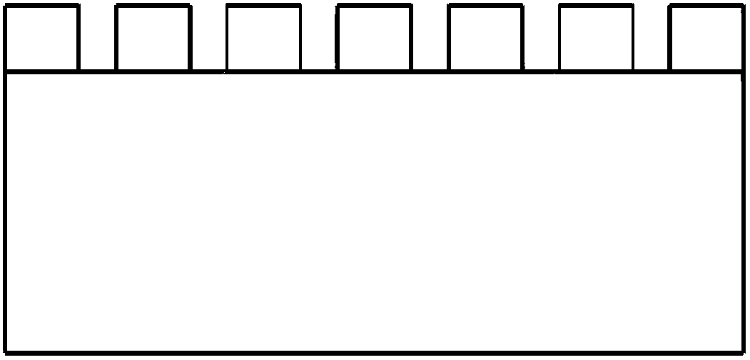
[0068] An infrared optical window with a three-step anti-reflection structure, the schematic diagram of which is shown in Figure 4 As shown, the top view is as Figure 5 As shown, the bottom view is as Figure 6 As shown, the infrared optical window is included, and the incident surface of the infrared optical window is etched with a three-step anti-reflection structure.

[0069] The infrared optical window material is one of silicon, germanium, zinc sulfide or zinc selenide.

[0070] The anti-reflection structure is a raised structure.

[0071] The protruding structure is one of cylinder, con...


PUM

PropertyMeasurementUnit
Thicknessaaaaaaaaaa

Abstract

The invention discloses an infrared optical window with a three-step anti-reflection structure. The window comprises an infrared optical window body, the incident plane of the infrared optical windowbody is etched with the three-step anti-reflection structure, a preparation method comprises the steps that silicon wafer is pretreated, a metal pattern mask is used for etching the three-step anti-reflection structure on a silicon plate, the structure includes an etching first step structure layer, an etching second step structure layer and an etching third step structure layer, the method for etching the anti-reflection structure adopts an induction coupled plasma etching machine and a combination process of etching and passivation, the etching gas is SF6, the passivation gas is C4F8, and inert gas He is added during etching and passivation. The structure can obviously increase the transmittance of the infrared window, improve the sensitivity of infrared devices, and reduce influence ofthe height of a step structure, structural parameters and the variation of a step period and depth on the transmittance, and the preparation method improves process tolerance of device manufacturing,and reduces the difficulty of craft production.

Description

technical field [0001] The invention belongs to the field of infrared optical windows, and in particular relates to an infrared optical window with a three-step anti-reflection structure and a preparation method thereof. Background technique [0002] The material of the traditional infrared optical window has a large reflection coefficient, which leads to the need for surface anti-reflection treatment to improve the window transmittance when used as an infrared optical window. The existing method to improve the transmittance is to coat the surface. According to different requirements, the number of coating layers is different, and it is divided into single-layer coating and multi-layer coating. Due to the coating process, there are various problems in the coating layer, such as adhesion, corrosion resistance, stability, thermal expansion mismatch, component penetration and diffusion, and the inability to find materials that match the required transmittance, etc. Inherent pr...

Claims


Application Information

Patent Timeline
IPC IPC(8): G02B1/118
CPCG02B1/118
Inventor 何少伟陈志祥陈定辉范文聪
Owner UNIV OF ELECTRONIC SCI & TECH OF CHINA
Learn More