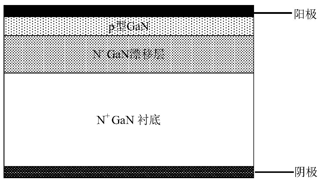
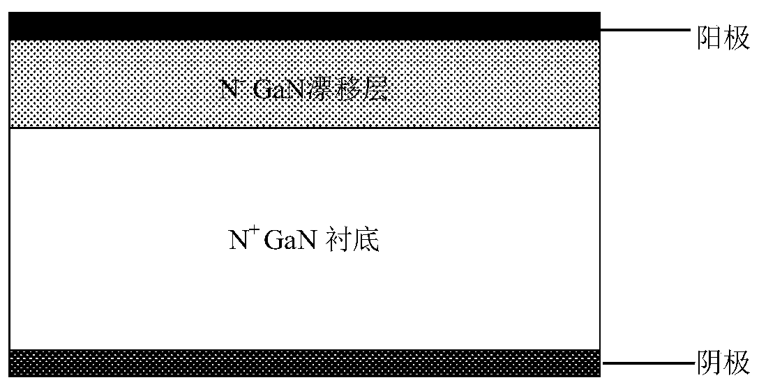
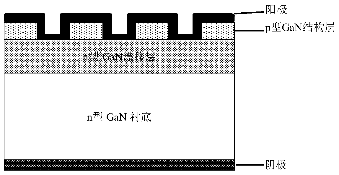
High-voltage gan-based JBS diode based on gradient drift region and manufacturing method thereof
A diode and high-voltage-resistant technology, which is applied in the field of power devices, GaN-based diode device structure and production, can solve the problems of high breakdown voltage, small turn-on voltage, short reverse recovery time, etc., and reduce the quantum tunneling effect , improve the breakdown voltage, high repeatability effect
- Summary
- Abstract
- Description
- Claims
- Application Information
AI Technical Summary
Problems solved by technology
Method used
Image
Examples
Embodiment 1
[0046] Example 1, making p-type graded Al composition Al y GaN structure layer and n-type graded Al composition Al x GaN structure layers, GaN-based JBS diodes with a thickness of 0.1 μm.
[0047] Step 1: Doping the GaN substrate material, such as Figure 5 (a) shown.
[0048] Do Si element doping on the GaN substrate material with a thickness of 200 μm, and set SiH 4 The flow rate is 5000sccm, and the doping concentration is 1×10 18 cm -3 n-type GaN substrate.
[0049] Step 2: Grow GaN drift layer, such as Figure 5 (b) shown.
[0050] GaN drift layer is epitaxially grown on the surface of n-type GaN substrate using MOCVD equipment, and the doping source is SiH 4 , set SiH 4 The flow rate is 50sccm, the time is 210min, the thickness is 3μm, and the doping concentration is 2×10 16 cm -3 Si-doped n-type GaN drift layer.
[0051] Step 3: Growing n-type Al x GaN structure layers, such as Figure 5 (c) shown.
[0052] Epitaxial growth of Al on n-type GaN drift layer...
Embodiment 2
[0063] Example 2, making p-type graded Al composition Al y GaN structure layer and n-type graded Al composition Al x GaN structure layers, GaN-based JBS diodes with a thickness of 0.3 μm.
[0064] Step 1: Doping the GaN substrate material with a thickness of 300 μm with Si element to obtain a doping concentration of 1×10 18 cm -3 n-type GaN substrate, the flow of doping is the same as step 1 of embodiment 1, such as Figure 5 (a) shown.
[0065] Step 2: growing a GaN drift layer, such as Figure 5 (b) shown.
[0066] GaN drift layer is epitaxially grown on the surface of n-type GaN substrate using MOCVD equipment, and the doping source is SiH 4 , set SiH 4 The flow rate is 150sccm, the time is 420min, the thickness is 6μm, and the doping concentration is 6×10 16 cm -3 Si-doped n-type GaN drift layer.
[0067] Step 3: Growing n-type Al x GaN structure layers, such as Figure 5 (c) shown.
[0068] Epitaxial growth of Al on n-type GaN drift layer using MOCVD equipmen...
Embodiment 3
[0079] Example 3, making p-type graded Al composition Al y GaN structure layer and n-type graded Al composition Al x GaN structure layers, GaN-based JBS diodes with a thickness of 0.5 μm.
[0080] Step A: doping the GaN substrate material with a thickness of 400 μm with Si element, setting SiH 4 The flow rate is 5000sccm, and the doping concentration is 1×10 18 cm -3 n-type GaN substrates, such as Figure 5 (a) shown.
[0081] Step B: Setting up SiH 4 The flow rate is 250sccm, the time is 560min, and the epitaxial growth thickness is 8μm on the surface of the n-type GaN substrate using MOCVD equipment, and the doping concentration is 10×10 16 cm -3 Si-doped n-type GaN drift layer, such as Figure 5 (b) shown.
[0082] Step C: Setting up SiH 4 The flow rate is 5000sccm, the time is 35min, and Al is epitaxially grown on the n-type GaN drift layer using MOCVD equipment x The GaN structure layer is obtained with a thickness of 0.5 μm and a doping concentration of 2×10 ...
PUM
| Property | Measurement | Unit |
|---|---|---|
| thickness | aaaaa | aaaaa |
| thickness | aaaaa | aaaaa |
| thickness | aaaaa | aaaaa |
Abstract
Description
Claims
Application Information
 - R&D
- Intellectual Property
- Life Sciences
- Materials
- Tech Scout
- Unparalleled Data Quality
- Higher Quality Content
- 60% Fewer Hallucinations
Browse by: Latest US Patents, China's latest patents, Technical Efficacy Thesaurus, Application Domain, Technology Topic, Popular Technical Reports.
© 2025 PatSnap. All rights reserved.Legal|Privacy policy|Modern Slavery Act Transparency Statement|Sitemap|About US| Contact US: help@patsnap.com


