
Electromagnetic shielding film with high absorption performance and preparation method thereof

An electromagnetic shielding, high absorption technology, applied in the fields of magnetic/electric field shielding, chemical instruments and methods, electrical components, etc., can solve the problems of acid and alkali resistance, high density, poor wave absorbing performance, etc. Simple process and low price effect

Pending Publication Date: 2018-06-29
SOUTH CHINA UNIV OF TECH
View PDF5 Cites 4 Cited by
  • Summary
  • Abstract
  • Description
  • Claims
  • Application Information

AI Technical Summary

Problems solved by technology

[0004] The purpose of the present invention is to solve the problems of poor wave-absorbing performance, acid and alkali resistance, and high density of current electromagnetic shielding materials, and to provide an electromagnetic shielding film with simple molding, low cost, and high absorption performance and a preparation method thereof, which can make the film possess Good shielding performance and good absorbing performance

Method used


Image

  • Electromagnetic shielding film with high absorption performance and preparation method thereof
  • Electromagnetic shielding film with high absorption performance and preparation method thereof

Examples


Embodiment 1

[0031] A highly absorbent electromagnetic shielding film such as figure 1 As shown, the electromagnetic shielding film 3 has a multi-layer structure, including six layers of insulating adhesive layer 1 and five layers of chopped carbon fiber felt absorbing layer 2, wherein any two layers of adjacent chopped carbon fiber felt absorbing layer 2 They are bonded together through an insulating adhesive layer 1, and the outermost chopped carbon fiber felt wave-absorbing layer 2 uses the insulating adhesive layer 1 as a protective film.

[0032] The material of the insulating adhesive layer 1 is polycarbonate film.

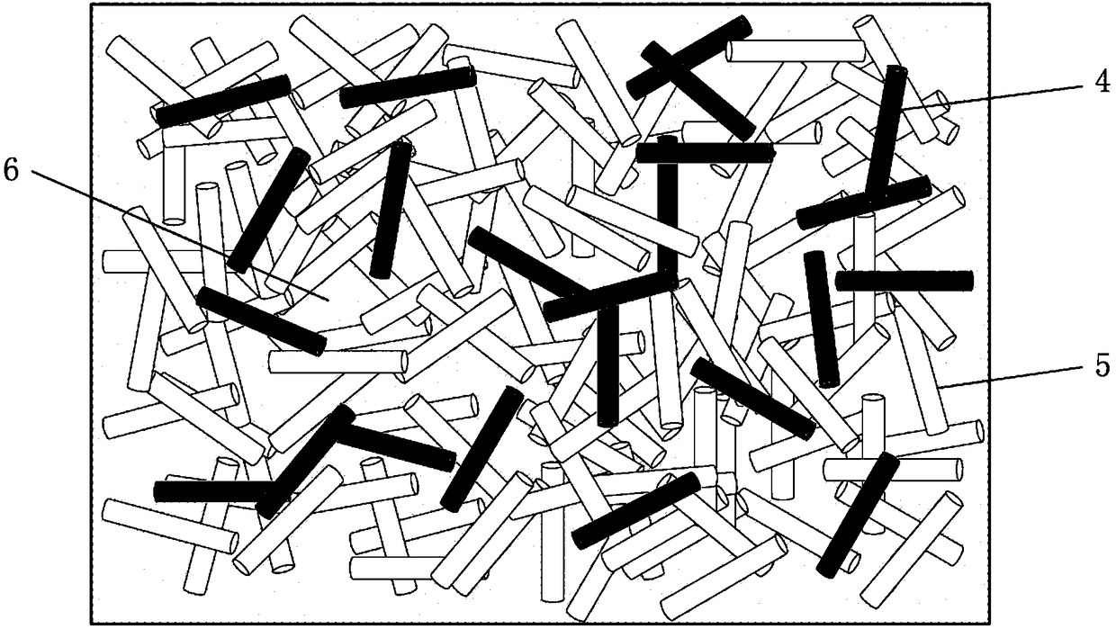
[0033] The structural representation of the chopped carbon fiber felt wave-absorbing layer 2 is as follows: figure 2 As shown, it is a chopped carbon fiber mat with a carbon fiber content of 6wt%, which is prepared from chopped carbon fiber 4 and ES fiber 5 by wet papermaking technology.

[0034] The preparation method of the electromagnetic shielding film with high a...

Embodiment 2

[0040] A highly absorbent electromagnetic shielding film such as figure 1 As shown, the electromagnetic shielding film 3 has a multi-layer structure, including six layers of insulating adhesive layer 1 and five layers of chopped carbon fiber felt absorbing layer 2, wherein any two layers of adjacent chopped carbon fiber felt absorbing layer 2 They are bonded together through an insulating adhesive layer 1, and the outermost chopped carbon fiber felt wave-absorbing layer 2 uses the insulating adhesive layer 1 as a protective film.

[0041] The material of the insulating adhesive layer 1 is polycarbonate film.

[0042] The structural representation of the chopped carbon fiber felt wave-absorbing layer 2 is as follows: figure 2 As shown, it is a chopped carbon fiber mat with a carbon fiber content of 5wt%, which is prepared from chopped carbon fiber 4 and ES fiber 5 by wet papermaking technology.

[0043]The preparation method of the electromagnetic shielding film with high ab...

Embodiment 3

[0049] An electromagnetic shielding film with high absorption performance, having a multi-layer structure, including eight layers of insulating adhesive layer 1 and seven layers of chopped carbon fiber felt absorbing layer 2, wherein any two adjacent layers of chopped carbon fiber felt absorb wave The layers 2 are bonded together by an insulating adhesive layer 1, and the outermost chopped carbon fiber felt wave-absorbing layer 2 uses the insulating adhesive layer 1 as a protective film.

[0050] The material of the insulating adhesive layer 1 is polycarbonate film.

[0051] The chopped carbon fiber mat wave-absorbing layer 2 is a chopped carbon fiber mat with a carbon fiber content of 4wt%, which is prepared from chopped carbon fibers 4 and ES fibers 5 by wet papermaking technology.

[0052] The preparation method of the electromagnetic shielding film with high absorption performance of the present invention can specifically be realized through the following steps:

[0053] ...


PUM

PropertyMeasurementUnit
lengthaaaaaaaaaa
thicknessaaaaaaaaaa
thicknessaaaaaaaaaa

Abstract

The invention discloses an electromagnetic shielding film with high absorption performance and a preparation method thereof. The electromagnetic shielding film provided by the invention is provided with a multi-layer structure, and comprises insulated bonding layers and chopped carbon fiber felt wave-absorbing layers, wherein any two adjacent chopped carbon fiber felt wave-absorbing layers are bonded into a whole through one insulated bonding layer; and the outermost chopped carbon fiber felt wave-absorbing layer adopts one insulated bonding layer as a protective film. The chopped carbon fiberfelt wave-absorbing layers have relatively low shielding performance and excellent wave-absorbing performance. The chopped carbon fiber felt wave-absorbing layers and the insulated bonding layer aresuperposed to perform hot-pressing forming, so that shielding performance of the material is improved. The electromagnetic shielding film has the advantages of being high in mechanical strength, goodin softness, small in density, high in electromagnetic shielding property, high in wave-absorbing performance, and the like, and has a wide application prospect in the important fields such as electromagnetic radiation protective systems and antiradar systems.

Description

technical field [0001] The invention relates to fields requiring wave-absorbing technology, such as military aviation and precision electronic equipment, in particular to an electromagnetic shielding film with high absorption performance and a preparation method thereof. Background technique [0002] The increasing number of electronic devices has brought great convenience to human beings, but at the same time, the electromagnetic waves generated by these devices are also threatening human life. Electromagnetic waves radiated by electronic devices can interfere with the normal operation of other electronic devices, causing electromagnetic interference problems. Moreover, electromagnetic waves are extremely harmful to human health. Long-term exposure to electromagnetic waves can lead to serious health problems such as headaches, sleep disorders, and even cancer. [0003] At present, metal materials are commonly used electromagnetic shielding materials. Due to the excellent ...

Claims


Application Information

Patent Timeline
Patent Type & Authority Applications(China)
IPC IPC(8): B32B9/02B32B9/04B32B27/02B32B27/12B32B7/12B32B3/24B32B27/36B32B37/00B32B37/06B32B37/10B32B37/12B32B38/18B29D7/01H05K9/00
CPCH05K9/0088B29D7/01B32B3/266B32B5/08B32B5/26B32B7/12B32B27/12B32B27/365B32B37/003B32B37/06B32B37/10B32B37/12B32B38/1808B32B2262/106B32B2262/14B32B2250/42B32B2262/0253B32B2250/05B32B2307/558B32B2307/206B32B2307/212B32B2307/102
Inventor 陆龙生汤伟津邢迪汤勇
Owner SOUTH CHINA UNIV OF TECH
Learn More