Constant-current device and manufacturing method thereof
A technology of constant current devices and manufacturing methods, applied to semiconductor devices, electrical components, transistors, etc., to achieve the effects of saving chip area, strong constant current capability, and stable current value
- Summary
- Abstract
- Description
- Claims
- Application Information
AI Technical Summary
Problems solved by technology
Method used
Image
Examples
Embodiment 1
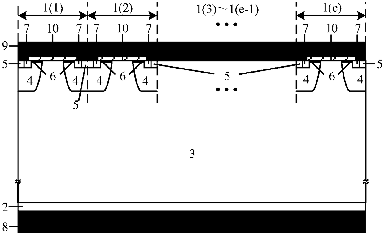
[0062] Such as Figure 4 As shown, a constant current device includes two parts: a cell area and a terminal area. The cell area includes a plurality of cells 1(1), 1(2)...1(e) with the same structure and sequentially connected , each cell includes a P-type doped substrate 2, an N-type epitaxial layer 3, and a diffused P-type well region 4 located in the N-type epitaxial layer 3. The diffused P-type well region 4 is two and located respectively At both ends of each cell, the first P-type heavily doped region 5 and the N-type heavily doped region 7 located in the diffused P-type well region 4, the first P-type heavily doped region 5 is located in the N-type heavily doped region On both sides of the impurity region 7, a first oxide layer 10 is provided on the upper surface of the N-type epitaxial layer 3 and the diffused P-type well region 4, and an N-type consumption layer is arranged between the upper surface of the diffused P-type well region 4 and the first oxide layer 10. T...
Embodiment 2
[0067] Such as Figure 5 As shown, the difference between this embodiment and Embodiment 1 is that: the terminal region includes a P-type doped region 21 formed around the groove by thermal process after the groove implantation.
[0068] The manufacturing method of the constant current device: the constant current device introduces a groove in the terminal region, and performs P-type impurity implantation around the groove to form a P-type doped region 21, so that the cell region and the device edge defect Phase isolation is achieved by PN junction isolation to achieve forward constant current and reverse high voltage resistance.
[0069] The manufacturing method of the constant current device specifically includes the following steps:
[0070] Step 1: using a P-type silicon wafer as a P-type doped substrate 2;
[0071] Step 2: performing N-type doped epitaxy on the P-type doped substrate 2;
[0072] Step 3: Etching a deep groove in the terminal area of the epitaxial wafe...
Embodiment 3
[0107] As shown in FIG. 9 (1)-(9), the manufacturing method of the constant current device provided by this embodiment, compared with FIG. 8, FIG. 9 omits the slot injection, and directly fills the slot with a medium.
[0108] The initial silicon wafer is epitaxy with one side as the front side, and then the terminal area is processed, including ring implantation, deep groove etching, groove side wall implantation, thick field oxygen in the growth groove and the upper surface of the terminal area, etc.; then, the junction is pushed to form a diffusion P-type well region; after pre-oxidation, perform channel adjustment implantation to form a surface depletion channel, then perform N-type heavily doped implantation, P-type heavily doped implantation, etch the redundant oxide layer; then deposit the oxide layer on the front side, Metal layer and passivation; then perform P-type heavily doped back implant; finally deposit metal layer and passivation on the back.
PUM
 Abstract
Description
Claims
Application Information
 - R&D
- Intellectual Property
- Life Sciences
- Materials
- Tech Scout
- Unparalleled Data Quality
- Higher Quality Content
- 60% Fewer Hallucinations
Browse by: Latest US Patents, China's latest patents, Technical Efficacy Thesaurus, Application Domain, Technology Topic, Popular Technical Reports.
© 2025 PatSnap. All rights reserved.Legal|Privacy policy|Modern Slavery Act Transparency Statement|Sitemap|About US| Contact US: help@patsnap.com


