Constant current device and manufacturing method thereof
A technology of constant current device and manufacturing method, applied in semiconductor/solid-state device manufacturing, semiconductor device, electrical components and other directions, to achieve the effect of simple manufacturing process, increased flexibility, and saving chip area
- Summary
- Abstract
- Description
- Claims
- Application Information
AI Technical Summary
Problems solved by technology
Method used
Image
Examples
Embodiment 1
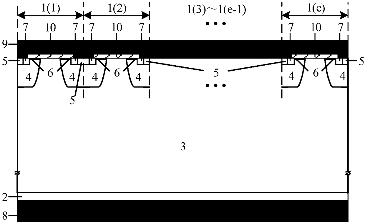
[0080] A constant current device, including a plurality of cells with the same structure and sequentially connected, each cell includes a P-type heavily doped substrate 2, an N-type doped epitaxial layer 3, and is located in the N-type doped epitaxial layer 3 The diffused P-type well region 4, the diffused P-type well region 4 is two and respectively located at both ends of each cell, the first P-type heavily doped region 5 and N located inside the diffused P-type well region 4 Type heavily doped region 7, the first P type heavily doped region 5 is located on both sides of the N type heavily doped region 7, an oxide layer 10 is provided on the upper surface of the N type doped epitaxial layer 3 and the diffused P type well region 4, The cell also includes a metal cathode 9 covering the entire upper surface of the cell, a metal anode 8 located on the lower surface of the P-type heavily doped substrate 2, the first P-type heavily doped region 5, the N-type heavily doped region 7 ...
Embodiment 2
[0099] Such as Figure 8 As shown, the difference between this embodiment and Embodiment 1 is that the constant current device also includes a P-type doped ring region 41 located at the inner edge of the cell region, and a diffused P-type well region 4 and a P-type well region at the outermost edge of the entire device. The doped ring region 41 is connected as a whole.
[0100] In this embodiment, there is no dielectric 13 inside the deep dielectric trench 12 for filling the gap of the oxide layer in the trench.
[0101] As shown in FIG. 7(1)-(9), FIG. 7 is a schematic flow chart of the manufacturing method of the constant current device provided in this embodiment. Among them, (1) is the initial silicon wafer; (2) is the silicon wafer after N-type doped epitaxy on the front side; (3) is etching a deep groove in the end area of the epitaxial wafer; (4) is performing P-type Impurity implantation; (5) Thick field oxygen and inner wall of the groove for the growth terminal re...
Embodiment 3
[0103] Such as Figure 4 As shown, the difference between this embodiment and Embodiment 3 is that: the dielectric deep groove 12 is provided with a dielectric 13 for filling the gap of the oxide layer in the groove.
[0104] Further, in the constant current device, in addition to polysilicon, other filling materials, such as silicon, silicon dioxide, etc., are used to fill the oxide layer gap in the groove, and it is even possible not to fill the oxide layer gap in the groove, that is, to fill The thing is air.
[0105] As a preferred manner, each doping type in the constant current device is correspondingly changed to opposite doping, that is, when P-type doping changes to N-type doping, N-type doping changes to P-type doping.
[0106] As a preferred manner, the semiconductor material used in the constant current device is silicon or silicon carbide.
[0107] Further, the P-type doped ring region 41 in the constant current device can be one or more according to the differe...
PUM
| Property | Measurement | Unit |
|---|---|---|
| Length | aaaaa | aaaaa |
| Thickness | aaaaa | aaaaa |
Abstract
Description
Claims
Application Information
 - R&D
- Intellectual Property
- Life Sciences
- Materials
- Tech Scout
- Unparalleled Data Quality
- Higher Quality Content
- 60% Fewer Hallucinations
Browse by: Latest US Patents, China's latest patents, Technical Efficacy Thesaurus, Application Domain, Technology Topic, Popular Technical Reports.
© 2025 PatSnap. All rights reserved.Legal|Privacy policy|Modern Slavery Act Transparency Statement|Sitemap|About US| Contact US: help@patsnap.com


