A method for manufacturing large-scale non-splicing micro-nano molds
A mold manufacturing, large-size technology, applied in the field of large-size non-splicing micro-nano mold manufacturing, to achieve the effects of high efficiency, low manufacturing cost and simple process
- Summary
- Abstract
- Description
- Claims
- Application Information
AI Technical Summary
Problems solved by technology
Method used
Image
Examples
Embodiment 1
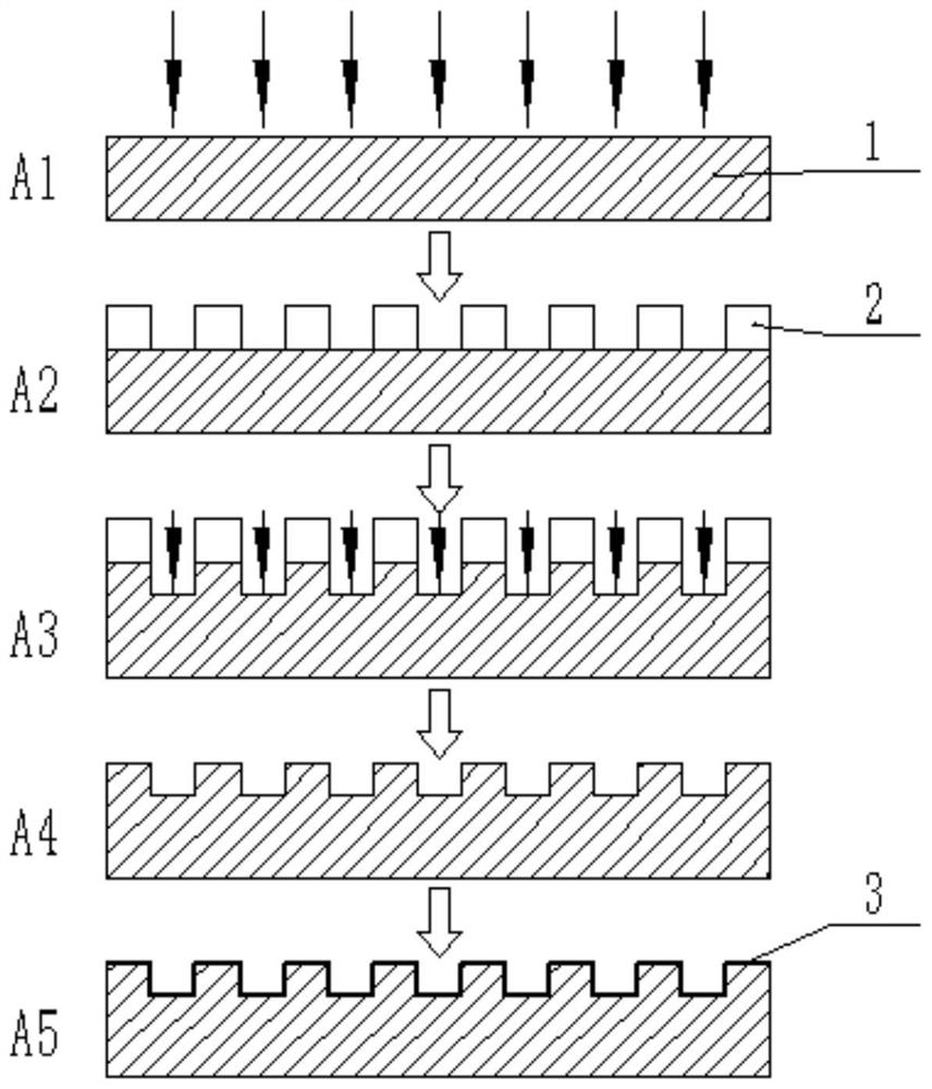
[0046] In this embodiment, a large-area sacrificial structure 2 is manufactured by thermal fusion electrohydrodynamic jet printing, and then the sacrificial structure 2 is transferred to a silicon substrate through an etching process, and the manufactured pattern structure is a wire grid structure. manufacturing process such as figure 1 As shown, the specific preparation steps include:
[0047] (1) Substrate 1 pretreatment: A1 plasma bombardment treatment of silicon substrate
[0048] Single crystal silicon or polycrystalline silicon is used as the substrate 1 (base). In order to improve the adhesion of the printed sacrificial structure 2 to the silicon substrate, a plasma treatment machine was used to conduct plasma bombardment treatment on the surface of the silicon substrate to improve the anti-adhesion performance of the silicon substrate.
[0049] (2) Manufacture of sacrificial structure 2: A2 uses thermal fusion electrohydrodynamic jet printing to manufacture sacrificial...
Embodiment 2
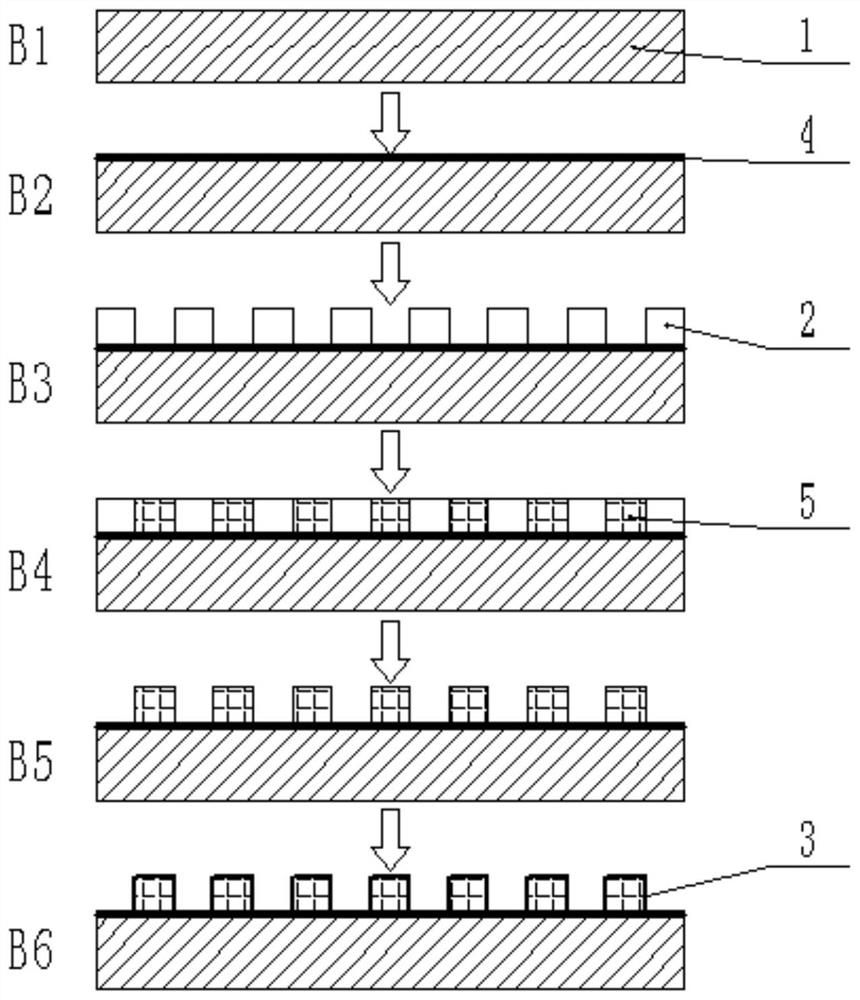
[0059] In this embodiment, the sacrificial structure 2 is manufactured by thermal fusion electrohydrodynamic jet printing, and then the sacrificial structure 2 is replicated through the electroforming process, and a large-sized micro-nano nickel mold without splicing is produced. The manufacturing process is as follows figure 2 As shown, the specific preparation steps include:
[0060] (1) Substrate 1 pretreatment: B1 ultrasonically cleans the glass substrate
[0061] Electrohydrodynamic jet printing substrate 1 pre-printed with glass as hot melt. The glass substrate was ultrasonically cleaned for 30 min, and then blown dry with nitrogen.
[0062] (2) Sputtering seed layer: B2 sputters a seed layer of about 100nm on the printed glass substrate
[0063] An electroformed seed layer 4 of Cr / Cu with a thickness of about 100 nm is sputtered on the glass substrate.
[0064] (3) Fabrication of sacrificial structure 2 by hot-melt electrohydrodynamic jet printing: B3 uses hot-melt ...
PUM
 Abstract
Description
Claims
Application Information
 - R&D
- Intellectual Property
- Life Sciences
- Materials
- Tech Scout
- Unparalleled Data Quality
- Higher Quality Content
- 60% Fewer Hallucinations
Browse by: Latest US Patents, China's latest patents, Technical Efficacy Thesaurus, Application Domain, Technology Topic, Popular Technical Reports.
© 2025 PatSnap. All rights reserved.Legal|Privacy policy|Modern Slavery Act Transparency Statement|Sitemap|About US| Contact US: help@patsnap.com


