Semiconductor structure and its forming method, and sram

A technology of semiconductor and gate structure, which is applied in the direction of semiconductor devices, semiconductor/solid-state device manufacturing, transistors, etc., can solve the problems of poor overall performance of semiconductor devices, and achieve the goal of improving read redundancy, improving performance, and improving overall performance Effect

Active Publication Date: 2020-06-09
SEMICON MFG INT (SHANGHAI) CORP +1
View PDF4 Cites 0 Cited by
  • Summary
  • Abstract
  • Description
  • Claims
  • Application Information

AI Technical Summary

Problems solved by technology

[0004] However, the performance of the static random access memory in the semiconductor device formed by the prior art needs to be further improved, so that the overall performance of the semiconductor device is relatively poor

Method used


Image

  • Semiconductor structure and its forming method, and sram
  • Semiconductor structure and its forming method, and sram
  • Semiconductor structure and its forming method, and sram

Examples


Embodiment Construction

[0015] It can be seen from the background art that the performance of static random access memory (SRAM) in semiconductor structure needs to be improved.

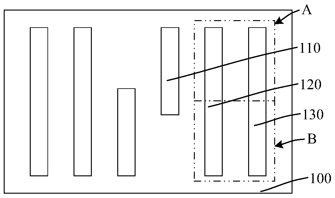
[0016] For SRAM, it mainly includes a pull-up (Pull Up, PU) transistor, a pull-down (Pull Down, PD) transistor, and a transfer gate (Pass Gate, PG) transistor, and the read margin of the memory has a significant impact on the memory. Performance plays a key role. If the read redundancy performance of the memory can be improved, the performance and yield of the memory will be improved, and the overall performance of the semiconductor device will be improved accordingly. Wherein, the read redundancy of the memory is proportional to the beta ratio (betaratio), and the beta ratio is the ratio between the on-state current (Ion) of the pull-down transistor and the on-state current of the pass-gate transistor.

[0017] Therefore, increasing the on-state current of the pull-down transistor or reducing the on-state current of the pa...


PUM


Abstract

A semiconductor structure and method for forming the same, and SRAM, the method comprising: providing a base, including a substrate and discrete fins located on the substrate, the substrate including a transfer gate transistor region; forming a gate structure across the fins , and the gate structure covers part of the top surface and sidewall surface of the fin; the transfer gate doping region is formed in the fins on both sides of the gate structure of the transfer gate transistor region, and the transfer gate doping region on at least one side adopts the method of conducting the fin part Formed by ion-doped non-epitaxial layer. The transmission gate doping region on at least one side of the present invention is formed by ion-doping the non-epitaxial layer of the fin. Compared with the scheme of forming the transmission gate doping region by epitaxial layer on both sides, the present invention increases the subsequent metal The contact resistance between the silicide and the doped region of the transmission gate reduces the on-state current of the formed transmission gate transistor; the SRAM beta ratio is inversely proportional to the on-state current of the transmission gate transistor, so that the read redundancy of the SRAM is improved.

Description

technical field [0001] The invention relates to the field of semiconductors, in particular to a semiconductor structure, a forming method thereof, and an SRAM. Background technique [0002] In the current semiconductor industry, integrated circuit products can be mainly divided into three types: logic, memory and analog circuits, among which memory devices account for a considerable proportion of integrated circuit products. With the development of semiconductor technology, storage devices are more widely used, and the storage device and other device regions need to be formed on a chip at the same time to form an embedded semiconductor storage device. For example, to embed the storage device in the central processing unit, it is necessary to make the storage device compatible with the embedded central processing unit platform, and maintain the specifications and corresponding electrical performance of the original storage device. [0003] Generally, the memory device needs ...

Claims


Application Information

Patent Timeline
Patent Type & Authority Patents(China)
IPC IPC(8): H01L29/78H01L29/06H01L27/11
CPCH01L29/0603H01L29/0684H01L29/7855H10B10/12H01L21/823418H01L21/823431H01L29/66795H01L29/41791H01L29/7851H01L27/0924H01L29/0847H01L29/165H10B99/00G11C11/4023H01L27/0886
Inventor 李勇
Owner SEMICON MFG INT (SHANGHAI) CORP
Why Eureka
Try Eureka