Metal interconnect structure and fabrication method thereof

A technology of metal interconnection structure and fabrication method, applied in semiconductor/solid-state device manufacturing, electrical components, circuits, etc., can solve problems such as affecting yield, short circuit of aluminum lining, and unclean etching

Active Publication Date: 2020-10-27
SHANGHAI HUALI MICROELECTRONICS CORP
View PDF4 Cites 0 Cited by
  • Summary
  • Abstract
  • Description
  • Claims
  • Application Information

AI Technical Summary

Problems solved by technology

[0011] In the above metal interconnection process, photomask technology is used in steps 2, 5, and 7, and the process flow is cumbersome. At the same time, because aluminum is used as a liner, its critical dimension is large, and the thickness of aluminum deposition is also relatively thick.
The thicker the aluminum liner, the greater the stress on the aluminum liner. After the aluminum liner is deposited, the whisker defect on the surface of the aluminum liner will also intensify. When the size of the whisker defect is large enough, it will lead to relative Short circuit adjacent to the aluminum pad, and in the subsequent metallization pattern etching process, the etching is not clean, affecting the yield

Method used


Image

  • Metal interconnect structure and fabrication method thereof
  • Metal interconnect structure and fabrication method thereof
  • Metal interconnect structure and fabrication method thereof

Examples


Embodiment Construction

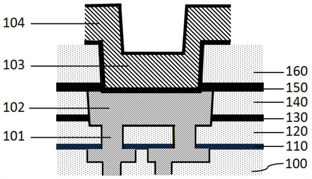
[0041] As described in the background technology, the existing metal interconnection structure manufacturing method has a cumbersome process flow. At the same time, because aluminum is used as a pad, its critical dimension is relatively large, and the thickness of aluminum deposition is also relatively thick. Whisker-shaped defects on the surface of the aluminum pad ( whiskerdefect) will also be exacerbated. When the size of the whisker-shaped defect is large enough, it will cause a short circuit of the adjacent aluminum pad, and in the subsequent metallization pattern etching process, the etching will not be clean and affect the yield.

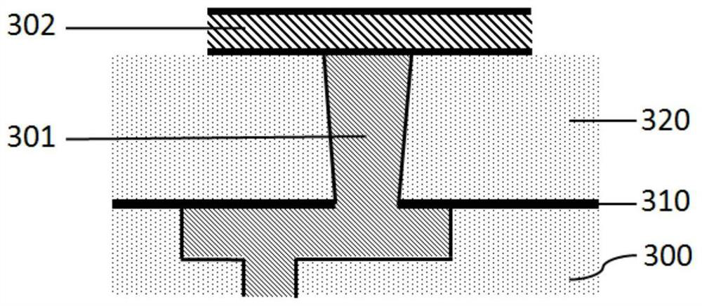
[0042] Considering that metal aluminum can also be used as a metal connection, and exhibits excellent performance under a certain line width, the aluminum liner layer can be used as both a liner and a top metal layer in a metal interconnection structure.

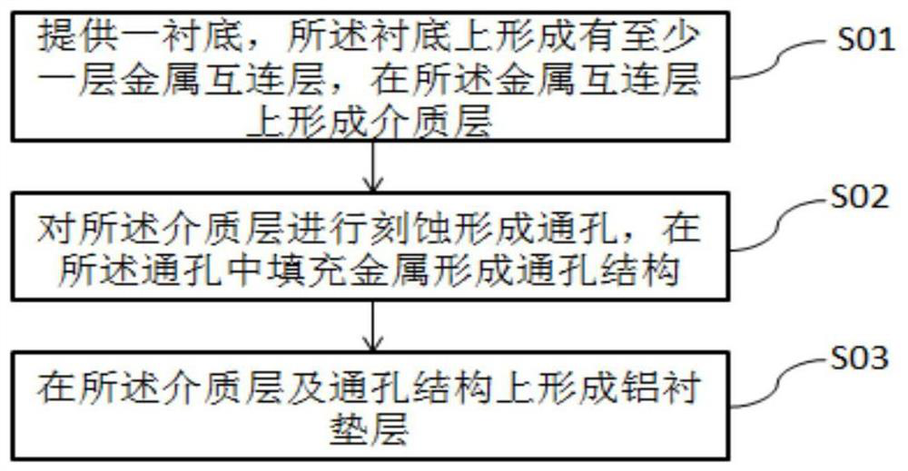
[0043] The invention provides a method for manufacturing a metal interconnection structu...


PUM

PropertyMeasurementUnit
thicknessaaaaaaaaaa

Abstract

The invention provides a metal interconnection structure and a manufacturing method thereof. At least one metal interconnection layer is formed on a substrate, a dielectric layer is formed on the metal interconnection layer and is etched to form a through hole, the through hole is filled with metal to form a through hole structure, and an aluminum lining layer is formed on the dielectric layer andthe through hole structure. The aluminum lining layer can serve as a lining as well as a top metal layer, the top metal layer and a re-distributed through hole layer can be omitted, technical processis simplified, and the production cost is reduced. The aluminum lining layer is thinner, whisker defects in the surface of the aluminum lining layer are reduced, and influence on subsequent technologies is reduced.

Description

technical field [0001] The invention relates to the field of semiconductor manufacturing, in particular to a metal interconnection structure and a manufacturing method thereof. Background technique [0002] In the semiconductor back-end process, a multi-layer metal interconnection structure can be provided on the semiconductor substrate according to different needs. Each layer of metal interconnection structure includes a metal interconnection line and an insulating layer, and trenches and via holes are formed in the insulating layer. Then metal is deposited in the groove and the through hole, and the deposited metal is the metal interconnection, and copper is generally selected as the material of the metal interconnection. Then an aluminum pad is deposited on the basis of the above structure, and the top layer interconnection structure is bonded to the aluminum pad to prepare for the subsequent packaging process. [0003] In the existing metal interconnection structure, th...

Claims


Application Information

Patent Timeline
Patent Type & Authority Patents(China)
IPC IPC(8): H01L21/768
CPCH01L21/76802H01L21/76843H01L21/76877H01L21/76895
Inventor 王贺莹黄冠群陈广龙
Owner SHANGHAI HUALI MICROELECTRONICS CORP
Why Eureka
Try Eureka