


Quick Research
Generate reliable direction feasibility study reports for your R&D in just a few steps.

Technical Q&A
Discover and master advanced knowledge NOW. Basics, ideas, possibilities, all at once.

Find Solutions
As an expert in R&D theories, this can generate solutions to your technical problems instantly.

Evaluate Feasibility
Analyze your overall solution with one click, know your potential R&D risks in advance.

Monitor Landscape
Get weekly tech updates, stay abreast of the latest tech innovations and key insights.
SRAM reading-writing circuit and SRAM data accessing method
A technology for writing data and circuits, applied in the field of reading and writing SRAM circuits and SRAM data access, it can solve problems such as the impact of control clock quality, speed bottlenecks, clock skew, etc., to overcome sampling timing problems, improve operating frequency, and ensure clock quality effect
- Summary
- Abstract
- Description
- Claims
- Application Information
AI Technical Summary
Problems solved by technology
Method used
Image

Examples
Embodiment 1
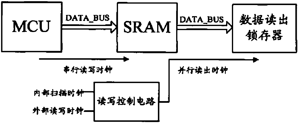
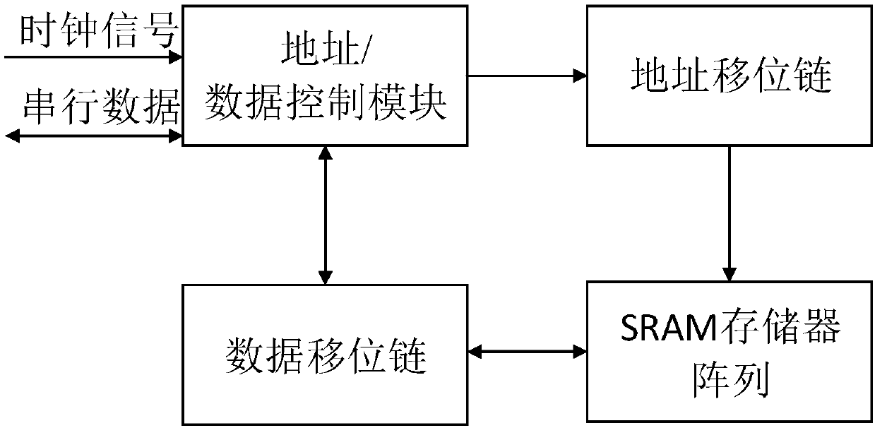
[0044] See figure 2 , image 3 and Figure 4 , figure 2 A schematic circuit diagram of a read-write SRAM provided by an embodiment of the present invention, image 3 A schematic diagram of a circuit structure of a read-write SRAM provided by an embodiment of the present invention, Figure 4 It is a flowchart of a method for reading and writing an SRAM provided by an embodiment of the present invention. .
[0045] The circuit includes: an address / data control module (Ad / Data control), an address shift chain (AddressShift Chain, abbreviated as ASC), a data shift chain (Data Shift Chain, abbreviated as DSC) and an SRAM memory array, wherein,
[0046] The address / data control module receives a clock signal (Clock, abbreviated as Clk) and serial data (Serial_data), and is used to decode the serial data in the clock signal and output a shift enable signal;
[0047] The address shift chain is connected to the address / data control module, and is used to receive the shift enabl...
Embodiment 2
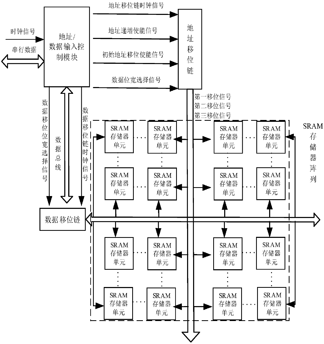
[0074] see again image 3 , this embodiment specifically describes the circuit for reading and writing SRAM of the present invention on the basis of the foregoing embodiments.
[0075] The address / data control module receives serial clock signals and serial data, wherein the initial address, data and instructions are all input to the address / data control module through the serial data interface;
[0076] The address / data control module transmits the clock signal of the address shift chain, the address increment enable signal and the initial address shift enable signal to the address shift chain, and the address / data control module controls the address shift chain to perform address shift operations. The shift chain transmits the address shift signal to the SRAM unit through the address shift bus, and performs an address shift increment operation through the address shift bus, and the address shift signal is determined by the data shift bit width selection signal.
[0077] Pre...
Embodiment 3
[0082] see again Figure 4 . This embodiment describes the method for reading and writing an SRAM of the present invention on the basis of the above embodiments. The specific method includes the following steps:
[0083] It mainly includes the following steps;
[0084] Step 1. Data loading;
[0085] Step 1.1, start the circuit and prepare for data reception;
[0086] Step 1.2, the address / data control module samples the received data according to the set data stream format and loads the initial address;
[0087] Step 1.3, the address / data control module loads the control instruction after the initial address is loaded.
[0088] Preferably, the control instructions include a single-row read instruction, a single-row write instruction, a read increment instruction, and a write increment instruction.
[0089] Step 2, the address / data control module judges whether to perform address increment;
[0090] Step 2.1, the address / data control module judges as no, then performs a ...
PUM
 Abstract
Description
Claims
Application Information
 - R&D Engineer
- R&D Manager
- IP Professional
- Industry Leading Data Capabilities
- Powerful AI technology
- Patent DNA Extraction
Browse by: Latest US Patents, China's latest patents, Technical Efficacy Thesaurus, Application Domain, Technology Topic, Popular Technical Reports.
© 2024 PatSnap. All rights reserved.Legal|Privacy policy|Modern Slavery Act Transparency Statement|Sitemap|About US| Contact US: help@patsnap.com