A kind of magnetic film material with perpendicular magnetic anisotropy and its preparation method
An anisotropic and magnetic thin film technology, applied in the direction of magnetic thin film, magnetic film to substrate application, magnetic objects, etc., can solve the problems of disappearance and reduction of perpendicular magnetic anisotropy of thin film materials
- Summary
- Abstract
- Description
- Claims
- Application Information
AI Technical Summary
Problems solved by technology
Method used
Image
Examples
preparation example Construction
[0031] Another object of the present invention is to provide a method for preparing the above-mentioned magnetic thin film material, which specifically includes the following steps:
[0032] Step 1: Select the base material and clean it;
[0033] Step 2: Co-sputtering method is used to deposit Ta and a semi-metallic element alloy compound deposited on the base material processed in step 1 as a buffer layer,
[0034] Step 3: Deposit Co / Pt (Pd, Ir, Au), Fe / Pt (Pd, Ir, Au), Pt / Co / MO, Pt / Fe / MO, CoFeB / MO on the buffer layer (MO is Multilayer films of metal oxides (such as MgO, AlOx, etc.);
[0035] Step 4: Co-sputtering method is used to deposit Ta and semi-metallic element alloy compounds deposited on Co / Pt (Pd, Ir, Au), Fe / Pt (Pd, Ir, Au), Pt / Co / MO, Pt / Fe / MO, CoFeB / MO (MO is a metal oxide such as MgO, AlOx) multilayer film as a protective layer;
[0036] Step 5: Combine the alloy compound of Ta and semimetal elements (such as B, Si, As, Sb, Te, Po) prepared above (0.1~100.0 nm) / (1.0~200...
Embodiment 1
[0043] The background vacuum degree of the sputtering chamber is 6.0×10 -5 Pa, pass 99.99% purity argon into the coating chamber for 0.5 hours before sputtering, and maintain the pressure at 0.6 Pa; during sputtering, the pressure of 99.99% purity high purity argon is 0.2 Pa; the substrate is cooled with circulating deionized water, parallel to A 16 kA / m magnetic field is applied to the plane of the substrate to induce an easy magnetization direction. Prepare a film with Ta as a buffer layer.
[0044] The film is annealed in a vacuum annealing furnace, the annealing temperature is 300℃, the annealing time is 30 m, and it is cooled with the furnace in a magnetic field. The background vacuum of the annealing furnace is 3.0×10 -5 Pa, apply a 55 kA / m magnetic field along the easy axis of the film during annealing.
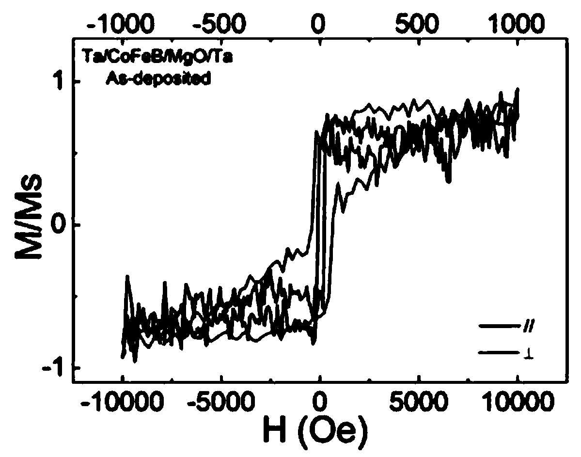
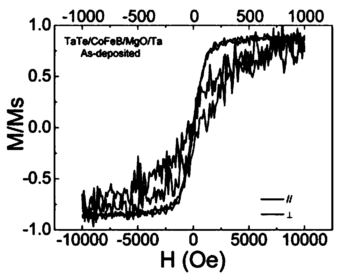
[0045] figure 1 The magnetization curve of Ta(5 nm) / CoFeB(1 nm) / MgO(2 nm) / Ta(2 nm) thin film as prepared figure 2 The magnetization curve of Ta(5 nm) / CoFeB(1 nm) / MgO(2 n...
Embodiment 2
[0047] The background vacuum degree of the sputtering chamber is 6.0×10 -5 Pa, pass 99.99% purity argon into the coating chamber for 0.5 hours before sputtering, and maintain the pressure at 0.6 Pa; during sputtering, the pressure of 99.99% purity high purity argon is 0.2 Pa; the substrate is cooled with circulating deionized water, parallel to A 16 kA / m magnetic field is applied to the plane of the substrate to induce an easy magnetization direction. The alloy compound of Ta and semimetal element Te is prepared by co-sputtering method. Through chemical analysis, the proportion of Ta in the alloy compound is controlled to be 85%, and the proportion of Te is 15%.
[0048] The film is annealed in a vacuum annealing furnace, the annealing temperature is 400℃, the annealing time is 30 m, and it is cooled with the furnace in a magnetic field. The background vacuum of the annealing furnace is 3.0×10 -5 Pa, apply a 55 kA / m magnetic field along the easy axis of the film during annealing....
PUM
| Property | Measurement | Unit |
|---|---|---|
| thickness | aaaaa | aaaaa |
| thermal stability | aaaaa | aaaaa |
| thickness | aaaaa | aaaaa |
Abstract
Description
Claims
Application Information
 - R&D
- Intellectual Property
- Life Sciences
- Materials
- Tech Scout
- Unparalleled Data Quality
- Higher Quality Content
- 60% Fewer Hallucinations
Browse by: Latest US Patents, China's latest patents, Technical Efficacy Thesaurus, Application Domain, Technology Topic, Popular Technical Reports.
© 2025 PatSnap. All rights reserved.Legal|Privacy policy|Modern Slavery Act Transparency Statement|Sitemap|About US| Contact US: help@patsnap.com


