GaN-based vertical cavity surface emitting light source with tunable light emitting wavelength

A technology of vertical cavity surface emission and light-emitting wavelength, which is applied in the direction of lasers, phonon exciters, laser components, etc., can solve the problems of device processing technology and difficult practical application in the process of complex material growth, and achieve simplified process and device production Difficulty, effect of increasing tuning range

Inactive Publication Date: 2018-03-30
XIAMEN UNIV
View PDF1 Cites 6 Cited by
  • Summary
  • Abstract
  • Description
  • Claims
  • Application Information

AI Technical Summary

Problems solved by technology

However, these require extremely complex material growth processes and device processing techniques, which are difficult to be practically applied.
And so far there is no report of a wavelength-tunable GaN-based surface-emitting light source.

Method used


Image

  • GaN-based vertical cavity surface emitting light source with tunable light emitting wavelength
  • GaN-based vertical cavity surface emitting light source with tunable light emitting wavelength
  • GaN-based vertical cavity surface emitting light source with tunable light emitting wavelength

Examples


Embodiment Construction

[0021] In order to make the object, technical solution and advantages of the present invention clearer, the process flow of the present invention will be further described in detail below in conjunction with the accompanying drawings.

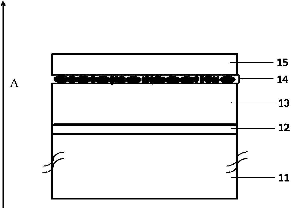
[0022] 1) if figure 1 As shown, the epitaxial layer with the quantum dot active region structure is grown on the sapphire substrate 11 by using the MOCVD method: the undoped u-GaN epitaxial layer 12, the n-type GaN epitaxial layer 13, and the SK mode growth InGaN / GaN Quantum dot active layer 14, p-type GaN epitaxial layer 15. InGaN quantum dots have different size distributions. exist figure 1 In , mark A is the material growth direction.

[0023] 2) to figure 1 The shown epitaxial wafer is used to make a tunable surface emitting light source device, and the cross-sectional structure of the device is shown in figure 2 shown. From bottom to top, the devices are: copper substrate 21 made by electroplating, lower dielectric film distributed...


PUM


Abstract

The invention discloses a GaN-based vertical cavity surface emitting light source with tunable light emitting wavelength, and relates to an emitting light source. The vertical cavity surface emittinglight source is provided with an epitaxial layer; the epitaxial layer comprises a substrate, a lower dielectric film distributed Bragg reflector, an ITO current expansion layer, a p type Cr / Au electrode, an SiO<2> current limiting layer, p type GaN, a quantum dot active layer, n type GaN, an n type Cr / Au electrode and an upper dielectric film distributed Bragg reflector from the bottom up in sequence. By taking quantum dots of different dimensions as the active layer, the tunable gain characteristic is obtained; by combination with a resonance cavity effect, the output characteristic of the light emitting wavelengths tunable between strong coupling modes can be obtained; the light emitting wavelength tuning ranges range from green-yellow light to purple light, so that large-range tuning isrealized; and compared with the conventional method for manufacturing a tunable light emitting device, complex material growth and period manufacturing process are not needed in the invention, so that the technological process and the device manufacturing difficulty are greatly simplified, and the tuning range of the light emitting wavelengths is expanded.

Description

technical field [0001] The invention relates to an emitting light source, in particular to a GaN-based vertical cavity surface emitting light source with tunable emission wavelength. Background technique [0002] GaN-based vertical cavity surface emitting light sources have broad application prospects in solid-state lighting, full-color display, high-density optical storage, medical treatment, multi-channel high-bandwidth optical communication, high-resolution printing, and biosensing. one of the research hotspots. The surface emitting light source has the advantages of small size, low threshold, circular symmetrical spot, and easy realization of single-mode lasing ([1] R. Shimada and H. Wide bandgap semiconductor-based surface-emitting lasers: recent progress in GaN-based vertical cavity surface-emitting lasers and GaN- / ZnO-based polariton lasers. Proc. IEEE 98(7), 1220-1233(2010)). But current research mainly focuses on fixed-wavelength light sources, that is, a device ...

Claims


Application Information

Patent Timeline
IPC IPC(8): H01S5/187H01S5/34H01S5/065
CPCH01S5/187H01S5/065H01S5/3412
Inventor 张保平梅洋许荣彬翁国恩应磊莹郑志威
Owner XIAMEN UNIV
Why Eureka
Try Eureka