A method for detecting fingerprint defects on the appearance of polycrystalline silicon solar cells

A solar cell and defect detection technology, which is applied in optical testing flaws/defects, measuring devices, and material analysis by optical means, etc., which can solve problems such as uneven image texture, increased production costs for enterprises, and detection difficulties.

Inactive Publication Date: 2021-01-08
HEBEI UNIV OF TECH +1
View PDF9 Cites 0 Cited by
  • Summary
  • Abstract
  • Description
  • Claims
  • Application Information

AI Technical Summary

Problems solved by technology

[0003] At present, the existing defect detection methods mainly rely on the traditional manual naked eye detection, which will be affected by subjectivity and visual fatigue, which will easily cause missed detection, false detection, and low efficiency. With the labor cost, the production cost of the enterprise will also increase.
Because polysilicon cells are affected by their own crystal lattice, the image texture on the surface is uneven, and defect feature extraction is difficult, which causes great troubles to the current defect detection. Therefore, the use of machine vision to detect cell defects has not been widely promoted.

Method used


Image

  • A method for detecting fingerprint defects on the appearance of polycrystalline silicon solar cells

Examples


Embodiment Construction

[0032] The following will clearly and completely describe the technical solutions in the embodiments of the present invention with reference to the accompanying drawings in the embodiments of the present invention. Obviously, the described embodiments are only some, not all, embodiments of the present invention. Based on the embodiments of the present invention, all other embodiments obtained by persons of ordinary skill in the art without making creative efforts belong to the protection scope of the present invention.

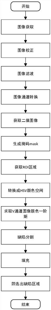
[0033] refer to figure 1 As shown, the present invention claims a method for detecting fingerprint defects on the appearance of solar cells, the method includes two steps:

[0034] The first step is to preprocess the image

[0035] 1-1 Image acquisition: calibrate the camera and eliminate distortion;

[0036] 1-2 Image correction: perform rotation correction processing on RGB three-channel images collected by industrial cameras;

[0037] 1-3 Image filtering...


PUM


Abstract

The invention provides a method for detecting appearance fingerprint defects of a polycrystalline silicon solar battery cell. The method is mainly divided into two steps: step 1, pre-processing the battery cell to obtain an interested region, wherein subsequent operation is carried out based on the interested region; step 2, identifying and marking a fingerprint region. The pre-processing step comprises the following steps: carrying out rotary correction operation on the collected battery cell so as to enable the battery cell to be parallel to a coordinate axis; then carrying out smooth processing to inhibit interference of image noises and high-frequency components; then converting an acquired RGB three-channel image into a gray level image; dividing a foreground region by adopting a fixed threshold value; then carrying out top hat conversion operation on the foreground region to eliminate interference of edges and a conveyor belt; taking an image subjected to top hat conversion processing as a mask so as to capture the interested region from the image subjected to the smooth processing.

Description

technical field [0001] The invention relates to the technical field of photovoltaic cell detection, and mainly relates to a method for detecting fingerprint defects on the appearance of polycrystalline silicon solar cells. Background technique [0002] The application of photovoltaic power generation is becoming more and more widespread. According to research, starting from 2030, solar photovoltaic power generation will increase by more than 10% every ten years in the world's total power supply, and by the end of the 21st century, renewable energy will account for more than 80% of the energy structure. , solar power generation accounted for more than 60%, solar power generation shows an important strategic significance. The production process of polycrystalline silicon solar cells is complicated, and various defects are prone to appear in the production process. After these defective cells are assembled, they not only affect the overall appearance, but also have a great impa...

Claims


Application Information

Patent Timeline
Patent Type & Authority Patents(China)
IPC IPC(8): G01N21/88G01N21/94
CPCG01N21/8806G01N21/8851G01N21/94G01N2021/8858G01N2021/8874G01N2021/888G01N2021/8887G01N2021/945
Inventor 陈海永张晓芳李爱梅胡洁王玉崔海根樊雷雷于矗卓
Owner HEBEI UNIV OF TECH
Why Eureka
Try Eureka