Preparation method of bottom emitting top gate self-aligning thin film transistor

A thin-film transistor and self-alignment technology, applied in transistors, semiconductor/solid-state device manufacturing, electric solid-state devices, etc., can solve problems such as low device mobility, exceeding the compensation range of compensation circuits, and poor stability

Pending Publication Date: 2018-03-16
BOE TECH GRP CO LTD
View PDF14 Cites 11 Cited by
  • Summary
  • Abstract
  • Description
  • Claims
  • Application Information

AI Technical Summary

Problems solved by technology

[0003] At present, in order to realize the characteristic of small parasitic capacitance required for higher-resolution OLED display, IGZO TFT adopts a top-gate self-aligned structure, but the main problem is how to reduce the distance between the channel region and the source-drain electrode. parasitic resistance, such as figure 1 As shown, the parasitic resistance R between the channel region A and the source and drain electrodes 01 P Including the resistance R of the LDD region (lowly doped drain region) B LDD and the contact resistance R between the source and drain electrodes 01 and the active layer 02 C ; The second is how to improve the light stability of the top-gate device. Since the oxide itself is sensitive to light, the electrical characteristics of the oxide material will change under light; in order to reduce the parasitic between the channel region A and the source-drain electrode 01 ...

Method used


Image

  • Preparation method of bottom emitting top gate self-aligning thin film transistor
  • Preparation method of bottom emitting top gate self-aligning thin film transistor
  • Preparation method of bottom emitting top gate self-aligning thin film transistor

Examples


Embodiment Construction

[0039] The following will clearly and completely describe the technical solutions in the embodiments of the present invention with reference to the accompanying drawings in the embodiments of the present invention. Obviously, the described embodiments are only some, not all, embodiments of the present invention. Based on the embodiments of the present invention, all other embodiments obtained by persons of ordinary skill in the art without making creative efforts belong to the protection scope of the present invention.

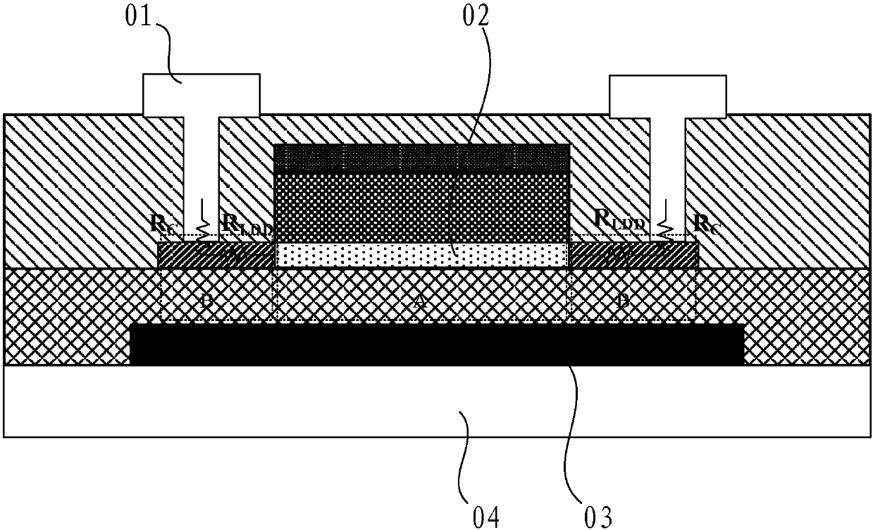
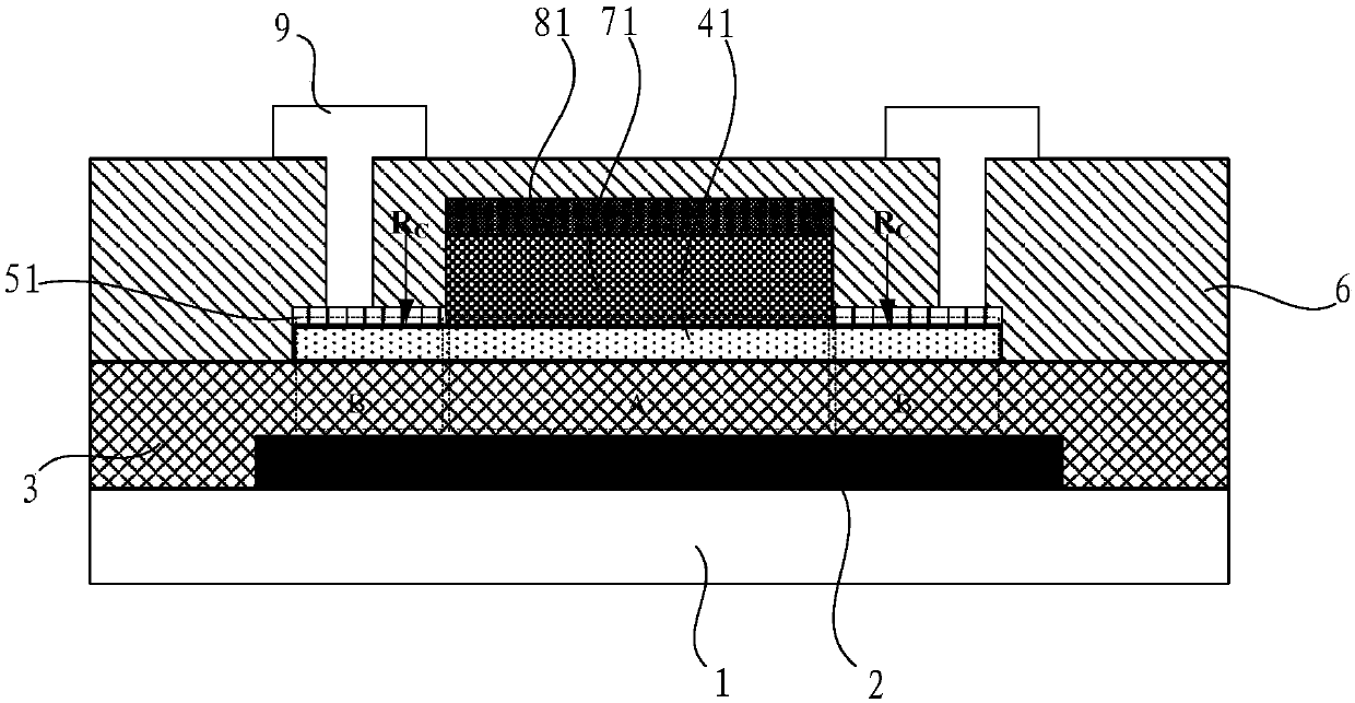
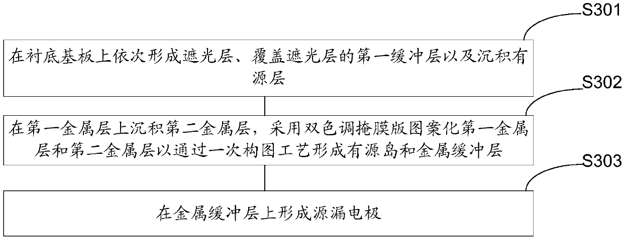
[0040] Such as figure 2 as well as image 3 As shown, a method for preparing a bottom-emitting top-gate self-aligned thin film transistor comprises the following steps:

[0041] Step S301, sequentially forming a light-shielding layer 2, a first buffer layer 3 covering the light-shielding layer 2, and depositing an active layer 4 on the base substrate 1;

[0042] Step S302, depositing the first metal layer 5 on the active layer 4, patterning the active layer...


PUM


Abstract

The invention relates to the technical field of display, and discloses a preparation method of a bottom emitting top gate self-aligning thin film transistor. The preparation method comprises the stepsthat a light shading layer, a first buffer layer covering the light shading layer and a deposited active layer which are formed on an underlying substrate in turn. The preparation method also comprises the steps that a first metal layer is deposited on the active layer, and the active layer and the first metal layer are patterned by using a two-tone mask plate so that an active island and a metalbuffer layer are formed through the primary composition process; and source and drain electrodes are formed on the metal buffer layer. The active layer does not need to be conductive, the parasitic resistance between the channel region and the source and drain electrodes can also be effectively reduced, and the number of the mask plate is not increased so that the technological process of the device can be simplified, the production cost can be saved, the metal buffer layer and the light shading layer are cooperated to effectively prevent the influence of the light on the channel region and the LDD region, the illumination stability of the top gate device can be improved, the problem of appearing of the residual image in display can be avoided and the efficiency of the technological process and the product yield rate can be enhanced.

Description

technical field [0001] The invention relates to the field of display technology, in particular to a method for preparing a bottom-emitting top-gate self-aligned thin film transistor. Background technique [0002] In the field of semiconductor technology, compared with traditional silicon-based thin film transistors (Si-TFTs), metal oxide thin film transistors represented by IGZO (indium gallium zinc oxide) TFTs (thin film transistors) are characterized by their high mobility, manufacturing process The advantages of simplicity, low cost, and large-area uniformity have been developed rapidly, and have become key devices for driving OLED (organic light-emitting diode) display panels. [0003] At present, in order to realize the characteristic of small parasitic capacitance required for higher-resolution OLED display, IGZO TFT adopts a top-gate self-aligned structure, but the main problem is how to reduce the distance between the channel region and the source-drain electrode. p...

Claims


Application Information

Patent Timeline
IPC IPC(8): H01L21/336H01L29/786H01L27/02
CPCH01L27/02H01L29/66742H01L29/786
Inventor 王国英宋振陈江博
Owner BOE TECH GRP CO LTD
Why Eureka
Try Eureka