Memory cells, methods of forming an array of two transistor-one capacitor memory cells, and methods used in fabricating integrated circuitry

A technology of memory cells and capacitors, applied in the direction of capacitors, transistors, circuits, etc., can solve problems such as incorporation and difficult capacitors

Active Publication Date: 2018-03-13
MICRON TECH INC
View PDF2 Cites 5 Cited by
  • Summary
  • Abstract
  • Description
  • Claims
  • Application Information

AI Technical Summary

Problems solved by technology

One of the limiting factors in the scalability of current 1T-1C configurations is the difficulty of incorporating capacitors with sufficiently high capacitance into highly integrated architectures

Method used


Image

  • Memory cells, methods of forming an array of two transistor-one capacitor memory cells, and methods used in fabricating integrated circuitry
  • Memory cells, methods of forming an array of two transistor-one capacitor memory cells, and methods used in fabricating integrated circuitry
  • Memory cells, methods of forming an array of two transistor-one capacitor memory cells, and methods used in fabricating integrated circuitry

Examples


Embodiment Construction

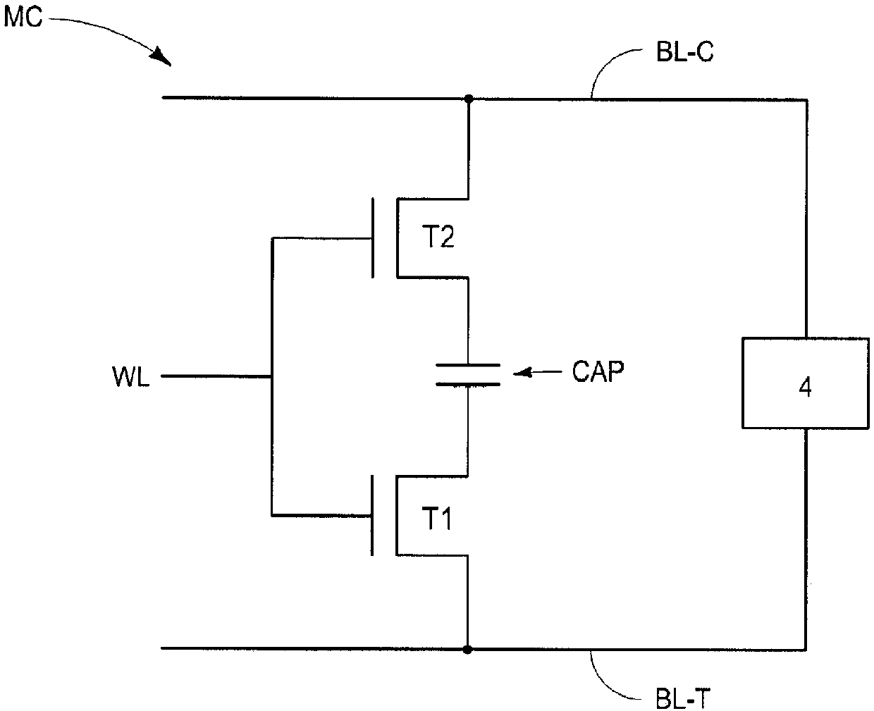
[0033]Embodiments of the invention include memory cells that are independent of fabrication methods. Embodiments of the invention also include methods of forming arrays of two transistor one capacitor (2T-1C) memory cells and methods for fabricating integrated circuits. While not in every way being so limited, the provided drawings depict fabrication methods and structures associated with 2T-1C memory cells, such as shown schematically in FIG. 1 . An example 2T-1C memory cell MC has two transistors T1 and T2 and a capacitor CAP. A source / drain region of T1 is connected to a first conductive node of capacitor CAP, and another source / drain region of T1 is connected to a first comparison bit line (eg, BL-T). The gate of T1 is connected to the word line WL. The source / drain region of T2 is connected to the second conductive node of the capacitor CAP, and the other source / drain region of T2 is connected to the second comparison bit line (eg, BL-C). The gate of T2 is connected to...


PUM


Abstract

The present invention relates to memory cells, methods of forming an array of two transistor-one capacitor memory cells, and methods used in fabricating integrated circuitry. A memory cell comprises first and second transistors laterally displaced relative one another. A capacitor is above the first and second transistors. The capacitor comprises a container-shape conductive first capacitor node electrically coupled with a first current node of the first transistor, a conductive second capacitor node electrically coupled with a first current node of the second transistor, and a capacitor dielectric material between the first capacitor node and the second capacitor node. The capacitor dielectric material extends across a top of the container-shape first capacitor node. Additional embodiments and aspects, including method, are disclosed.

Description

technical field [0001] Embodiments disclosed herein relate to memory cells, methods of forming memory cells, and methods for fabricating integrated circuits. Background technique [0002] Dynamic Random Access Memory (DRAM) is used in modern computing architectures. DRAM offers structural simplicity, low cost, and speed advantages over other types of memory. [0003] Currently, DRAMs typically have individual memory cells (so-called 1T-1C memory cells) that combine a capacitor with one of the transistor's source / drain regions, where the capacitor is coupled with one of the transistor's source / drain regions. One of the limiting factors in the scalability of current 1T-1C configurations is the difficulty of incorporating capacitors with sufficiently high capacitance into highly integrated architectures. Accordingly, it is desirable to develop new memory cell configurations suitable for incorporation into highly integrated modern memory architectures. [0004] While the pres...

Claims


Application Information

Patent Timeline
IPC IPC(8): H01L27/108H01L21/8242
CPCH10B12/39H10B12/033H01L28/90H01L28/60H10B12/01H10B12/03H10B12/05H10B12/485H10B53/30H01L21/76897H01L28/91
Inventor 斯科特·E·西里斯
Owner MICRON TECH INC
Why Eureka
Try Eureka