Al technical title is built by PatSnap Al team. It summarizes the technical point description of the patent document.
A transistor and isolation structure technology, applied in the field of LDMOS transistor structure, can solve problems such as avalanche breakdown of LDMOS structure
Active Publication Date: 2021-05-07
SEMICONDUCTOR MANUFACTURING INTERNATIONAL (BEIJING) CORP +1
View PDF3 Cites 0 Cited by
Summary
Abstract
Description
Claims
Application Information
AI Technical Summary
This helps you quickly interpret patents by identifying the three key elements:
Problems solved by technology
Method used
Benefits of technology
Problems solved by technology
[0006] In view of the above-mentioned shortcomings of the prior art, the purpose of the present invention is to provide an L-DMOS transistor structure for solving the problem that the LDMOS structure is prone to avalanche breakdown in the prior art
Method used
Image
Click on the blue label to locate the original text in one second.
Reading with bidirectional positioning of images and text.
Examples
Embodiment 1
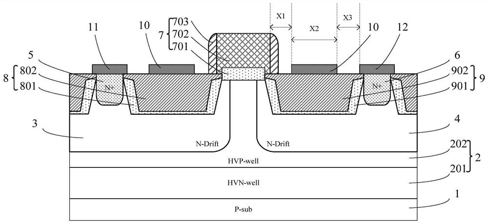
[0053] The present invention provides an LDMOS transistor structure, please refer to figure 1 , shown as a schematic cross-sectional structure of the LDMOS transistor structure, including:
[0054] semiconductor substrate 1;
[0055] a first drift region 3 and a second drift region 4 located in the semiconductor substrate 1 and arranged separately;
[0056] a source 5 located in the first drift region 3 and a drain 6 located in the second drift region 4;
[0057] a gate structure 7 located on the semiconductor substrate 1 and in contact with the first drift region 3 and the second drift region 4 on both sides;
[0058] A first isolation structure 8 located in the first drift region 3 and isolating the source 5 from the gate structure 7; located in the second drift region 4 and separating the drain 6 from the gate structure 7 A second isolation structure 9 isolated by the gate structure 7; wherein:
[0059] A floating field plate 10 is disposed on the first isolation struct...
Embodiment 2
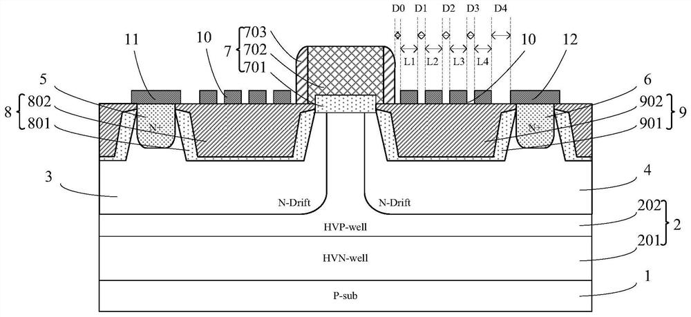
[0077] The difference between this embodiment and the first embodiment is that, in the first embodiment, a floating field plate 10 is respectively arranged on the first isolation structure 8 and the second isolation structure 9 . In this embodiment, the first isolation structure and the second isolation structure are both provided with a plurality of discrete floating field plates.
[0078] see figure 2 , which is a schematic cross-sectional structure diagram of the LDMOS transistor structure described in this embodiment, including:
[0079] semiconductor substrate 1;
[0080] a first drift region 3 and a second drift region 4 located in the semiconductor substrate 1 and arranged separately;
[0081] a source 5 located in the first drift region 3 and a drain 6 located in the second drift region 4;
[0082] a gate structure 7 located on the semiconductor substrate 1 and in contact with the first drift region 3 and the second drift region 4 on both sides;
[0083] A first i...
PUM
Abstract
The present invention provides an LDMOS transistor structure, comprising: a semiconductor substrate; a first drift region and a second drift region disposed separately in the semiconductor substrate; a source electrode located in the first drift region and a source electrode located in the semiconductor substrate. The drain in the second drift region; the gate structure located on the semiconductor substrate and in contact with the first drift region and the second drift region on both sides; located in the first drift region and a first isolation structure isolating the source from the gate structure; a second isolation structure located in the second drift region and isolating the drain from the gate structure; wherein: the first isolation Both the structure and the second isolation structure are provided with floating field plates. In the present invention, one or more floating field plates are arranged on the isolation structure between source-gate and drain-gate, which can increase the area of depletion region and reduce impact ionization, thereby obtaining higher breakdown voltage and saturated drain Current I dsat , and will not deteriorate the gate-to-drain capacitance C of the device gd and gate-source capacitance C gs .
Description
technical field [0001] The invention belongs to the field of semiconductor integrated circuits and relates to an LDMOS transistor structure. Background technique [0002] A liquid crystal display (Liquid Crystal Display, LCD) is a display device with a good development prospect at present, and more commonly used LCD devices are STN (super twisted type) and TFT (thin film transistor type). The process platform based on SPOCULL (Smic polycontact ultra low leakage) technology is aimed at the LCD driver market and has a good application prospect. The feature of SPOCULL technology is to replace the traditional metal connection by covering the active area with a polysilicon connection layer, which can achieve a smaller chip area. [0003] Lateral Diffusion MOS (LDMOS) transistors are widely used in power devices due to their high breakdown voltage and compatibility with CMOS processes. Compared with traditional MOS transistors, LDMOS devices have at least one isolation structure...
Claims
Application Information
Patent Timeline
Application Date:The date an application was filed.
Publication Date:The date a patent or application was officially published.
First Publication Date:The earliest publication date of a patent with the same application number.
Issue Date:Publication date of the patent grant document.
PCT Entry Date:The Entry date of PCT National Phase.
Estimated Expiry Date:The statutory expiry date of a patent right according to the Patent Law, and it is the longest term of protection that the patent right can achieve without the termination of the patent right due to other reasons(Term extension factor has been taken into account ).
Invalid Date:Actual expiry date is based on effective date or publication date of legal transaction data of invalid patent.
Patent Type & Authority Patents(China)
IPC IPC(8): H01L29/78H01L29/40
CPCH01L29/404H01L29/7816
Inventor 王伟江宇雷陈玉华魏琰
Owner SEMICONDUCTOR MANUFACTURING INTERNATIONAL (BEIJING) CORP