Transparent flexible GaN nanorod array light emitting diode device and manufacturing method thereof
A nanorod array and light-emitting diode technology, which is applied in the direction of electric solid-state devices, semiconductor devices, electrical components, etc., can solve the problems of irregular GaN nanorod arrays, failure to meet the requirements of transparency, and low efficiency, and achieve more lighting in the world , Illuminate the world beautifully, improve the effect of luminous efficiency
- Summary
- Abstract
- Description
- Claims
- Application Information
AI Technical Summary
Problems solved by technology
Method used
Image
Examples
preparation example Construction
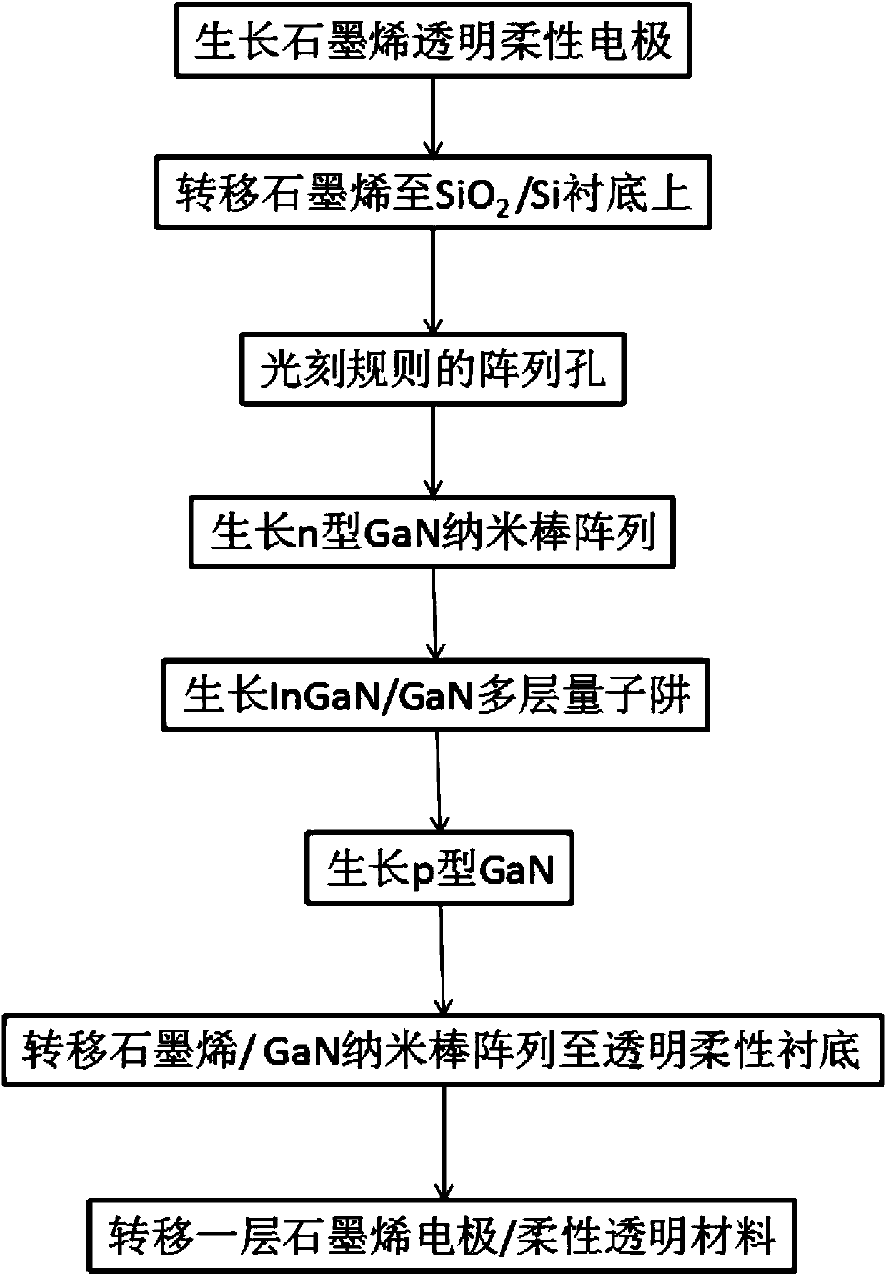
[0038] Such as figure 1 As shown, the preparation method of the transparent flexible GaN nanorod array light-emitting diode device comprises the following steps:
[0039] 1. The first transparent flexible electrode of single-layer graphene was prepared on a Cu substrate by chemical vapor deposition (CVD);
[0040] 2. Transfer graphene layer to SiO 2 / Si substrate;
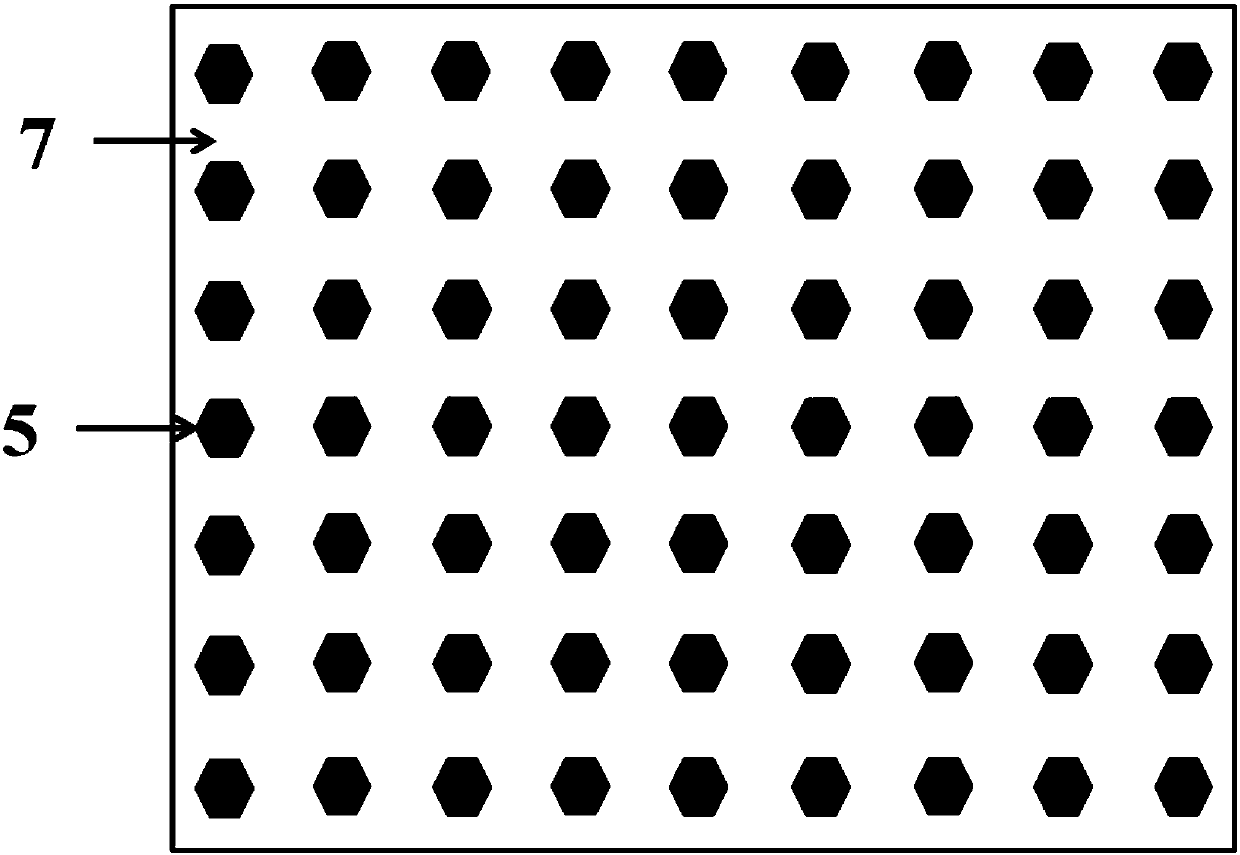
[0041] 3. A regular array of holes is etched by photolithography. The regular array holes are hexagonal, circular, square, triangular or rhombus, and the spacing of the holes is 30 nanometers to 5 microns.
[0042]4. Growth of GaN nanorod array LED structure in regular array holes: n-type GaN nanorod array, InGaN / GaN multilayer quantum well, p-type GaN, forming a composite structure; growing n-type GaN nanorod array, InGaN / GaN The methods of multilayer quantum wells and p-type GaN nanorod arrays are metal organic chemical vapor deposition (MOCVD), hydride vapor deposition (HVPE) or atomic layer deposition (ALD)...
Embodiment
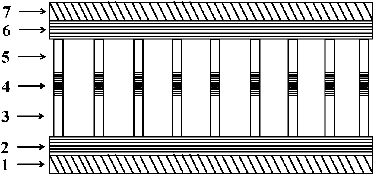
[0047] Such as Figure 1-Figure 4 As shown, the preparation method of the transparent and flexible GaN nanorod array light-emitting diode device in this embodiment, the specific steps are as follows:
[0048] 1) The first transparent flexible electrode 2 of single-layer graphene is grown on the Cu foil by chemical vapor deposition.
[0049] 2) Spin-coat a layer of polymethyl methacrylate (PMMA) on the graphene first transparent flexible electrode 2, and the thickness of PMMA is about 500 nanometers.
[0050] 3) Put the PMMA / graphene first transparent flexible electrode 2 / Cu foil into FeCl as a whole 3 Cu is etched away in aqueous solution (0.6mol / L).
[0051] 4) Clean and dry the silicon dioxide / silicon substrate, and transfer the first transparent flexible electrode 2 of PMMA / graphene to the side of the silicon wafer covered with silicon dioxide as a whole, and the thickness of the silicon dioxide layer is 100nm.
[0052] 5) Utilize acetone to remove PMMA.
[0053] 6) A l...
PUM
| Property | Measurement | Unit |
|---|---|---|
| Thickness | aaaaa | aaaaa |
Abstract
Description
Claims
Application Information
 - R&D
- Intellectual Property
- Life Sciences
- Materials
- Tech Scout
- Unparalleled Data Quality
- Higher Quality Content
- 60% Fewer Hallucinations
Browse by: Latest US Patents, China's latest patents, Technical Efficacy Thesaurus, Application Domain, Technology Topic, Popular Technical Reports.
© 2025 PatSnap. All rights reserved.Legal|Privacy policy|Modern Slavery Act Transparency Statement|Sitemap|About US| Contact US: help@patsnap.com


