A low-power charge-trap memory based on graphene oxide quantum dots and its preparation method

A technology of graphene quantum dots and charge trapping, applied in the direction of electric solid-state devices, circuits, electrical components, etc., can solve the problems of high operating voltage and large power consumption, and achieve low power consumption, long-lasting data storage, and low cost effects

Active Publication Date: 2020-01-14
HEBEI UNIVERSITY
View PDF6 Cites 0 Cited by
  • Summary
  • Abstract
  • Description
  • Claims
  • Application Information

AI Technical Summary

Problems solved by technology

[0003] One of the objectives of the present invention is to provide a low-power charge-trap memory based on graphene oxide quantum dots, to overcome the problems of high operating voltage and high power consumption of charge-trap memories with existing structures, and to achieve good capacitance retention performance , low power consumption, low leakage current and low voltage operation

Method used


Image

  • A low-power charge-trap memory based on graphene oxide quantum dots and its preparation method
  • A low-power charge-trap memory based on graphene oxide quantum dots and its preparation method
  • A low-power charge-trap memory based on graphene oxide quantum dots and its preparation method

Examples


Embodiment 1

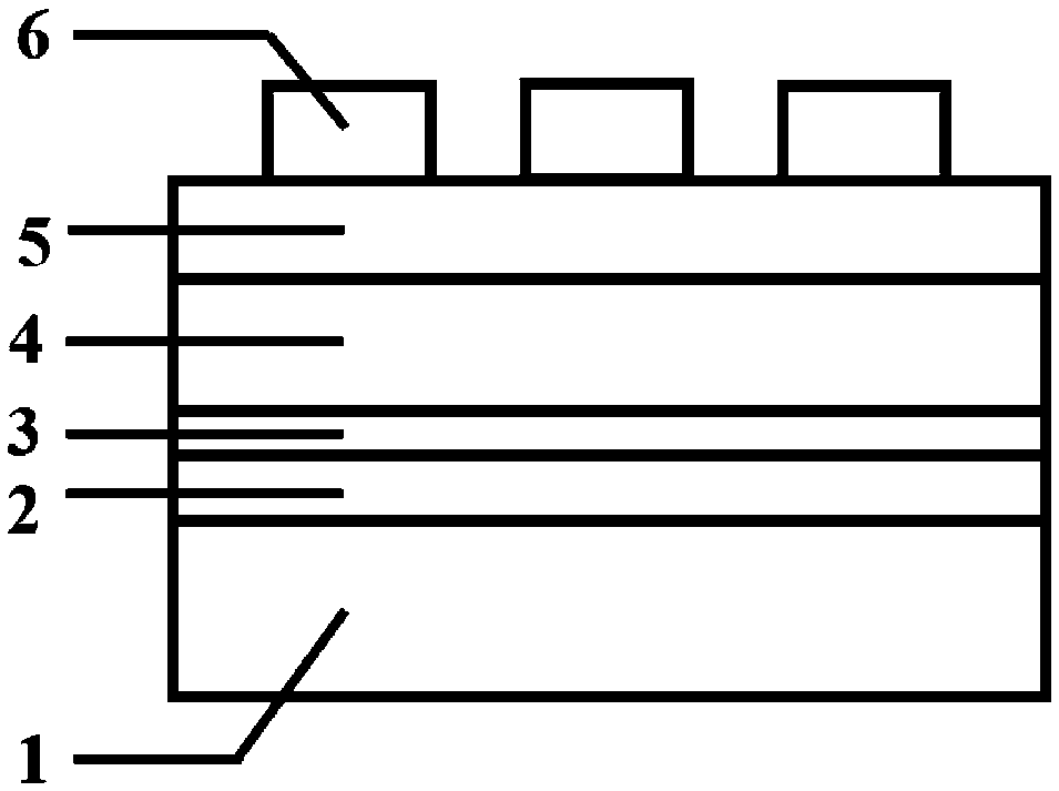
[0035] The charge trapping memory structure prepared by the present invention is as figure 1 As shown, its structure is that SiO is sequentially integrated on Si substrate 1 2 Tunneling layer 2, GQODs / Zr 0.5 Hf 0.5 o 2 Trapping layer, SiO 2 Barrier layer 5, Pd electrode film layer 6, GQODs / Zr 0.5 Hf 0.5 o 2 The trapping layer consists of GQODs layer 3 and Zr 0.5 Hf 0.5 o 2 layer 4, and the GQODs layer 3 is a single-layer graphene oxide quantum dot layer.

[0036] Si substrate 1 is p-type Si material with 100 crystal orientation; SiO 2 The thickness of tunneling layer 2 is 2~5nm; GQODs / Zr 0.5 Hf 0.5 o 2 The trapping layer 4 has a thickness of 5-80nm, preferably 10-40nm; SiO 2 The barrier layer 5 has a thickness of 5-50 nm, most preferably 5-20 nm; the Pd electrode film layer 6 is a circular electrode film with a thickness of 20-150 nm and a diameter of 60-300 μm.

Embodiment 2

[0038] The preparation method of the charge trapping memory of the present invention, the steps are as follows:

[0039] (a) The p-Si substrate was cleaned with ultrasonic waves in acetone, alcohol and deionized water in sequence, and then washed with HF solution (volume ratio H 2 O:HF=2:1) ​​wash for 2min, then ultrasonically clean with deionized water, take it out and use N 2 Blow dry; put the processed silicon substrate into a high-temperature annealing furnace, and anneal and grow SiO in an oxygen environment 2 Tunneling layer: first use 20s to rise from room temperature to 200°C, 60s to rise from 200°C to 500°C, keep at 500°C for 150s, 10s to drop to 100°C, 40s to drop from 100°C to room temperature, the obtained SiO 2 The thickness of the tunneling layer is 3nm, resulting in SiO 2 / Si structure substrate.

[0040] (c) SiO 2 The / Si structure substrate is placed on the rotating suction cup of the SC-1B homogenizer, and the rotation speed is set to 4000r / min. Use a rub...


PUM

PropertyMeasurementUnit
thicknessaaaaaaaaaa
thicknessaaaaaaaaaa
thicknessaaaaaaaaaa

Abstract

The invention provides a low-power charge-trap memory based on graphene oxide quantum dots and a preparation method thereof, the structure of which consists of Si substrate, SiO 2 Tunneling layer, GQODs / Zr 0.5 f 0.5 o 2 Trapping layer, SiO 2 Barrier layer and Pd top electrode; its preparation method: Si substrate is cleaned and corroded as substrate, and SiO is grown by high temperature annealing 2 For the tunneling layer, evenly throw a layer of GQODs on the tunneling layer SiO with SC-1B homogenizer 2 Above, the capture layer, barrier layer and electrode film layer are plated on the existing structure by magnetron sputtering. Compared with general charge-trap memory, this memory has the advantages of low operating voltage, good fatigue resistance, long-lasting data storage, large storage window, small charge leakage, low power consumption and low cost, and is very suitable for application in electronic equipment. , has a certain market application value.

Description

technical field [0001] The invention relates to a non-volatile memory device and a preparation method thereof, in particular to a low-power charge-trapping memory based on graphene oxide quantum dots and a preparation method thereof. Background technique [0002] The traditional Flash memory is a non-volatile memory, which consists of a silicon substrate, a tunneling layer, a floating gate layer, a barrier layer and a top electrode from bottom to top. Under the action of a certain bias voltage, the carriers in the substrate will tunnel through the oxide insulating layer and enter the floating gate layer. At this time, the metal floating gate is charged compared with before, and there are two completely different states of charged and uncharged. Realized the storage of information. Affected by Moore's Law, in order to miniaturize the device and scale it down, the tunneling layer has reached the physical limit of 7nm. Since the charge is evenly distributed in the floating ga...

Claims


Application Information

Patent Timeline
Patent Type & Authority Patents(China)
IPC IPC(8): H01L27/11563H01L27/11568
CPCH10B43/00H10B43/30
Inventor 闫小兵王宏张园园赵建辉周振宇
Owner HEBEI UNIVERSITY
Why Eureka
Try Eureka