Manufacturing method of parts of optical gratings of DFB laser

A DFB laser and manufacturing method technology, applied in the field of optoelectronics, can solve the problems of affecting the duty ratio of the grating, high requirements of the InP process, affecting the threshold current, output power and final yield, etc., so as to avoid the depth of the grating being too deep or too shallow. , Improve the output power and yield, improve the effect of manufacturing yield

Inactive Publication Date: 2018-02-23
WUHAN GUANGANLUN OPTOELECTRONICS TECH CO LTD
View PDF6 Cites 4 Cited by
  • Summary
  • Abstract
  • Description
  • Claims
  • Application Information

AI Technical Summary

Problems solved by technology

[0004] (1) Directly use reactive ion etching technology to etch off the material of the grating layer, and the etching depth of the grating on the chip is consistent. Etching damage, and the shape of the grating produced at the same time is rectangular, which is not conducive to the subsequent buried growth of the grating;
[0005] (2) Non-selective wet etching, usually using Br-based etching solution, can corrode InP and InGaAsP at the same time. Although it can form a grating morphology that is conducive to grating burial, non-selective etching will lead to lateral corrosion, which is harmful to corrosion. The requirements for process control are relatively high, and the consistency of the depth in the chip of wet etching is poor;
[0006] (3) Selective wet etching is adopted, and the InP layer in the grating layer is etched with HCl series etching solution, and then H 2 SO 4 A series of selective etching solutions are used to etch the InGaAsP layer in the grating layer. Although the consistency of the depth of the grating on the chip is good, the process requirements for the first selective etching of InP are relatively high, and the lateral etching of InP will eventually affect the thickness of the grating. Duty cycle, which in turn affects the threshold current, output power and final yield of DFB lasers

Method used


Image

  • Manufacturing method of parts of optical gratings of DFB laser
  • Manufacturing method of parts of optical gratings of DFB laser
  • Manufacturing method of parts of optical gratings of DFB laser

Examples


Embodiment Construction

[0034] The following will clearly and completely describe the technical solutions in the embodiments of the present invention with reference to the accompanying drawings in the embodiments of the present invention. Obviously, the described embodiments are only some, not all, embodiments of the present invention. Based on the embodiments of the present invention, all other embodiments obtained by persons of ordinary skill in the art without making creative efforts belong to the protection scope of the present invention.

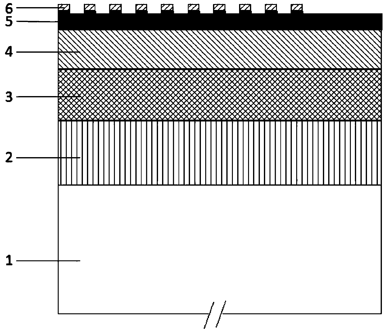
[0035] Such as Figure 1-Figure 4 , an embodiment of the present invention provides a method for fabricating a DFB laser partial grating, comprising the following steps:

[0036] Step 1: On the N-type indium phosphide substrate 1, the N-type InP buffer layer 2, the multi-quantum well structure 3, the P-type InP layer 4, the InGaAsP grating layer 5 and the InP grating layer are sequentially grown by metal-organic chemical vapor deposition method 6;

[0037] S...


PUM

PropertyMeasurementUnit
thicknessaaaaaaaaaa
thicknessaaaaaaaaaa
thicknessaaaaaaaaaa

Abstract

The invention provides a manufacturing method of parts of optical gratings of a DFB laser. The method comprises following steps of successively growing an N-type InP buffering layer, a multi-quantum well structure, a P-type InP layer, an InGaAsP optical grating layer and an InP optical grating layer on an N-type phosphatization indium substrate by use of the metallic organic chemical vapor deposition method; uniformly coating the surface of an epitaxial wafer with photoresist, shielding parts of the optical gratings through a photolithography mask, carrying out exposure under a photoetching machine and carrying out holographic exposure and development so as to form optical grating regions and non-optical grating regions; using the photoresist to serve as protection layers and corroding theInP optical grating layer in the optical grating layer by use of reactive ion etch technology; and using selective corrosion liquid for InGaAsP to corrode the InGaAsP optical grating layer and allowing the liquid to stand and corrode for 1-2 minutes under the indoor temperature. According to the invention, by using the photoresist to serve as protection layers and by use of the reactive ion etchtechnology and the selectivie wet etching, parts of optical gratings with the consistent depth are formed; and the method is suitable for batch manufacturing of DFB lasers.

Description

technical field [0001] The invention relates to the field of optoelectronic technology, in particular to a method for manufacturing a partial grating of a DFB laser. Background technique [0002] DFB lasers have been widely used in the field of optical fiber communication due to their good single-mode characteristics. Different single-mode wavelengths can be obtained by adjusting the grating period (usually 180-250nm) in the DFB laser, so as to meet the needs of optical fiber communication for different wavelengths. Therefore, the quality of grating fabrication in DFB lasers will determine the photoelectric characteristics and final yield of DFB lasers. [0003] Generally, there are two main methods for making lenticular graphics: holographic exposure and electron beam exposure. Holographic exposure is easy to manufacture, high in efficiency, and low in equipment cost, but it can only produce uniform gratings; while electron beam exposure can produce phase-shifted gratings...

Claims


Application Information

Patent Timeline
Patent Type & Authority Applications(China)
IPC IPC(8): H01S5/12H01S5/34G02B5/18
CPCH01S5/12G02B5/1857H01S5/34
Inventor 张恩许海明
Owner WUHAN GUANGANLUN OPTOELECTRONICS TECH CO LTD
Why Eureka
Try Eureka