OLED packaging structure and OLED packaging method

An encapsulation structure and encapsulation method technology, applied in the field of OLED, can solve the problems of destroying electrical properties and stability, OLED pixel luminous brightness changes, affecting OLED display quality, etc., to achieve the effects of improving life expectancy, good protection, and reducing impact

Inactive Publication Date: 2018-02-16
SHENZHEN CHINA STAR OPTOELECTRONICS SEMICON DISPLAY TECH CO LTD
View PDF6 Cites 11 Cited by
  • Summary
  • Abstract
  • Description
  • Claims
  • Application Information

AI Technical Summary

Problems solved by technology

[0006] There are certain disadvantages in the existing OLED packaging methods, which are mainly manifested in: in the process of curing the frame glue by UV light irradiation, due to the high energy of the UV tube, the TFT will generate carriers (electrons or space) under the UV light. hole), when the free carrier concentration increases, the threshold voltage (Vth) of the TFT will decrease, and the drift of Vth will directly cause the luminance of the OLED pixel to change, thus affecting the overall display quality of the OLED; that is, UV light irradiation will destroy the electrical properties and stability of the TFT in the TFT substrate

Method used


Image

  • OLED packaging structure and OLED packaging method
  • OLED packaging structure and OLED packaging method
  • OLED packaging structure and OLED packaging method

Examples


Embodiment Construction

[0031] In order to further illustrate the technical means adopted by the present invention and its effects, the following describes in detail in conjunction with preferred embodiments of the present invention and accompanying drawings.

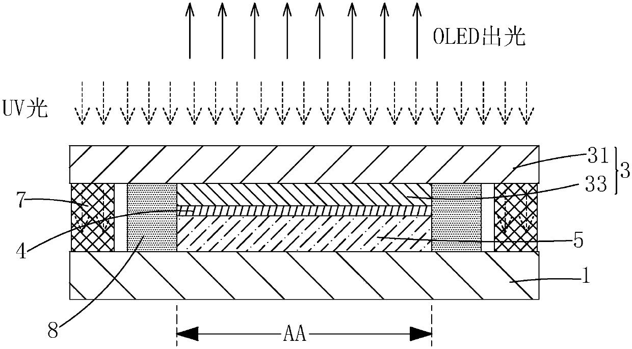
[0032] The invention provides an OLED packaging structure. figure 1 Shown is the first embodiment of the OLED packaging structure of the present invention, including a TFT substrate 1, a packaging cover 3 opposite to the TFT substrate 1, and a TFT substrate 1 close to the packaging cover in the effective display area AA of the OLED. The OLED device 5 on one side of the board 3 and the sealant 7 disposed between the TFT substrate 1 and the packaging cover 3 around the effective display area AA of the OLED.

[0033] The packaging cover plate 3 is improved compared with the prior art, and it includes a packaging substrate 31 and a UV blocking layer 33 disposed on the side of the packaging substrate 31 close to the TFT substrate 1 and correspondin...


PUM


Abstract

The invention provides an OLED packaging structure and an OLED packaging method. The OLED packaging structure comprises a TFT substrate (1), a packaging cover plate (3), an OLED device (5), and frameadhesive (7), wherein the packaging cover plate (3) is arranged opposite to the TFT substrate (1); the OLED device (5) is arranged in an effective display region (AA) of the OLED and on one side, close to the packaging cover plate (3), of the TFT substrate (1); the frame adhesive (7) is arranged on the periphery of the effective display region (AA) of the OLED and between the TFT substrate (1) andthe packaging cover plate (3); the packaging cover plate (3) comprises a packaging substrate (31) and an UV barrier layer (33) which is arranged on one side, close to the TFT substrate (1), of the packaging substrate (31) and corresponding to the effective display region (AA) of the OLED; and the UV barrier layer (33) is a transparent thin film with low UV light transmittance and high visible light transmittance, so that influence to the electrical performance and stability of the TFT in frame adhesive (7) curing process by UV light can be lowered, water vapor and oxygen are further isolated,and the service life of the OLED device (5) is prolonged.

Description

technical field [0001] The invention relates to the technical field of OLEDs, in particular to an OLED packaging structure and an OLED packaging method. Background technique [0002] Organic Light Emitting Diode (OLED) has self-illumination, low driving voltage, high luminous efficiency, short response time, high definition and contrast, nearly 180° viewing angle, wide operating temperature range, and can realize flexible display and large It has many advantages such as area full-color display, and is widely used in the fields of display, lighting, and smart wear. [0003] OLED devices are usually set on a thin film transistor array substrate (Thin Film Transistor Array Substrate, TFT Array Substrate, referred to as TFT substrate), including an anode, a hole injection layer, a hole transport layer, an organic light-emitting layer, an electron Transport layer, electron injection layer and cathode. The TFT in the TFT substrate is used as a switching device and a driving devi...

Claims


Application Information

Patent Timeline
Patent Type & Authority Applications(China)
IPC IPC(8): H01L51/52H01L51/56
CPCH10K50/84H10K71/00
Inventor 李文杰
Owner SHENZHEN CHINA STAR OPTOELECTRONICS SEMICON DISPLAY TECH CO LTD
Why Eureka
Try Eureka