


Quick Research
Generate reliable direction feasibility study reports for your R&D in just a few steps.

Technical Q&A
Discover and master advanced knowledge NOW. Basics, ideas, possibilities, all at once.

Find Solutions
As an expert in R&D theories, this can generate solutions to your technical problems instantly.

Evaluate Feasibility
Analyze your overall solution with one click, know your potential R&D risks in advance.

Monitor Landscape
Get weekly tech updates, stay abreast of the latest tech innovations and key insights.
Memristor with neural bionic function and preparation method and application
A bionic function and memristor technology, which is applied in the field of memristor with neuron bionic function and its preparation, can solve the problems of high operating voltage, small resistance change, large power consumption, etc., and achieve low operating voltage and resistance change. Large, low-power effects
- Summary
- Abstract
- Description
- Claims
- Application Information
AI Technical Summary
Problems solved by technology
Method used
Image

Examples
Embodiment 1
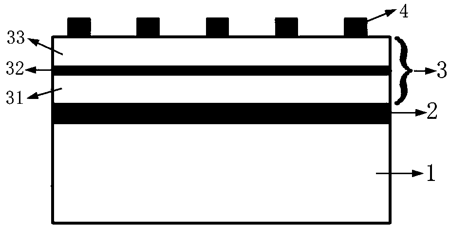
[0036] Such as figure 1 As shown, the memristor with neurobionic function provided by the present invention, its structure includes Pt / Ti / SiO 2 / Si substrate 1, in Pt / Ti / SiO 2 The Ag bottom electrode layer 2 formed on the Pt film layer of the Si substrate 1, the functional layer 3 formed on the Ag bottom electrode layer 2, and the Ag top electrode layer 4 formed on the functional layer 3. The functional layer 3 includes a first zirconium hafnium oxide film layer 31 , a graphene oxide quantum dot intermediate layer 32 and a second zirconium hafnium oxide film layer 33 from bottom to top. Among them, Pt / Ti / SiO 2 / The bottom of Si substrate 1 is the Si film layer, and the Si film layer is SiO 2 film, SiO 2 The Ti film layer is on the film layer, and the Pt film layer is on the Ti film layer. Therefore, the Pt film layer is Pt / Ti / SiO 2 / the topmost layer of the Si substrate 1 .
[0037] The thickness of the functional layer 3 is 10-20nm, wherein the thickness of the graphen...
Embodiment 2
[0048] (1) Pt / Ti / SiO 2 / Si substrate 1 is placed in a beaker filled with acetone, cleaned by ultrasonic waves for 10 minutes, then placed in a beaker filled with alcohol and cleaned by ultrasonic waves for 10 minutes, then taken out with clips and placed in a beaker filled with deionized water for ultrasonic cleaning 5min, then take it out and use nitrogen (N 2 ) and blow dry.
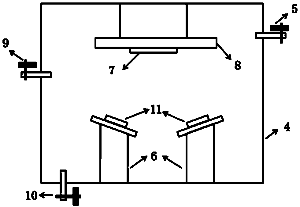
[0049] (2) using such as figure 2 For the magnetron sputtering equipment shown, open the cavity 4, take out the table 7, first polish it with sandpaper until it shines, clean the organic matter attached to the surface of the table with acetone, and finally wipe it clean with alcohol; put the cleaned Pt / Ti / SiO 2 / Si substrate 1 is placed on the table 7 for tableting, and the Pt / Ti / SiO is ensured during tableting 2 / Si substrate 1 is firmly pressed on the tablet press table 7 and flattened to ensure uniform film growth during sputtering. After the tablet press is completed, it is placed on the subst...
Embodiment 3
[0055] Embodiment 3 Performance testing of memristor
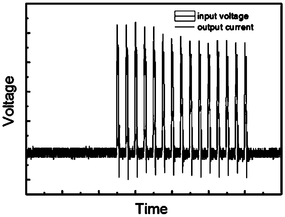
[0056] (1) The synapse simulation function of the device prepared in Example 2 was tested, and the results are shown in image 3 and Figure 4 shown. in image 3 It is a graph obtained by continuously applying 15 circles of 0.7v, 50ns pulse width square wave to the device. It can be seen from the graph that as the number of pulses increases, the current of the device increases gradually, and the resistance value decreases continuously. Figure 4 It is a picture obtained by continuously applying 15 circles of -0.7v, 50ns pulse width square wave to the device. It can be seen from the figure that as the number of pulses increases, the current of the device decreases gradually, and the resistance value increases continuously. pass image 3 and Figure 4 , indicating that the resistance of the memristive device is adjustable and has a good neurobiological effect.
[0057] (2) Paired pulse facilitation (PPF) in biological...
PUM
| Property | Measurement | Unit |
|---|---|---|
| thickness | aaaaa | aaaaa |
| thickness | aaaaa | aaaaa |
| thickness | aaaaa | aaaaa |
Abstract
Description
Claims
Application Information
 - R&D Engineer
- R&D Manager
- IP Professional
- Industry Leading Data Capabilities
- Powerful AI technology
- Patent DNA Extraction
Browse by: Latest US Patents, China's latest patents, Technical Efficacy Thesaurus, Application Domain, Technology Topic, Popular Technical Reports.
© 2024 PatSnap. All rights reserved.Legal|Privacy policy|Modern Slavery Act Transparency Statement|Sitemap|About US| Contact US: help@patsnap.com