Carbazole organic electroluminescent compound and organic light-emitting device thereof
A compound and luminescent technology, applied in organic chemistry, electrical solid devices, electrical components, etc., can solve the problems of high energy consumption, affecting device efficiency, poor thermal stability, etc., and achieve high luminous purity, high luminous efficiency, good The effect of thermal stability
- Summary
- Abstract
- Description
- Claims
- Application Information
AI Technical Summary
Problems solved by technology
Method used
Image
Examples
Embodiment 1
[0061] Synthesis of Compound 10
[0062]
[0063] In a flask, add Intermediate 2-1 (2g, 3.8mmol), 4-dianilinophenylboronic acid (1.2g, 4mmol), potassium carbonate (1.1g, 8mmol), palladium acetate (0.1g), X-phos (0.2g), dioxane (15mL), water (8mL), heated to reflux under nitrogen protection for 12 hours, cooled, extracted with dichloromethane, dried, and the crude product was purified by column chromatography to obtain 1.4g of product, product rate 49%.
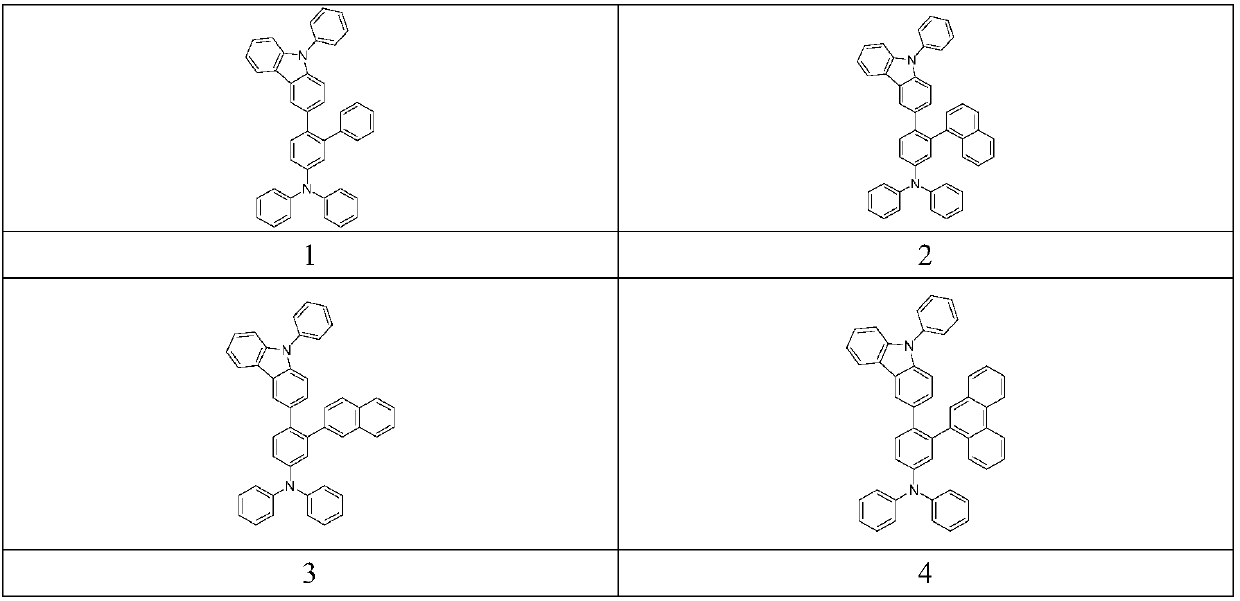
[0064] The synthesis of the final compound is the same as that of compound 10, and the raw materials and yields used are shown in Table 3:
[0065] table 3
[0066]
[0067]
[0068]
[0069]
Embodiment 16-30
[0071] Fabrication of Organic Electroluminescent Devices
[0072] Preparation of OLEDs using the compounds of the Examples
[0073] First, the transparent conductive ITO glass substrate 110 (with the anode 120 on it) (China CSG Group Co., Ltd.) is washed with deionized water, ethanol, acetone and deionized water in sequence, and then treated with oxygen plasma for 30 seconds.
[0074] Then, spin-coat PEDOT:PSS (polyethylenedioxythiophene: poly(styrene sulfonate)) with a thickness of 45 nm on the ITO as the hole injection layer 130, and dry at 150° C. for 30 minutes;
[0075] Then, on the hole injection layer, vapor-deposit the compound of the present invention with a thickness of 40 nm as the hole transport material 140,
[0076] Then, a luminescent layer 150 with a thickness of 30 nm is vapor-deposited on the electron blocking layer, wherein CBP is the main luminescent material, and 8% by weight of Ir(ppy) 3 As a phosphorescent doping guest material.
[0077] Then, 40 nm t...
PUM
| Property | Measurement | Unit |
|---|---|---|
| thickness | aaaaa | aaaaa |
Abstract
Description
Claims
Application Information
 - R&D
- Intellectual Property
- Life Sciences
- Materials
- Tech Scout
- Unparalleled Data Quality
- Higher Quality Content
- 60% Fewer Hallucinations
Browse by: Latest US Patents, China's latest patents, Technical Efficacy Thesaurus, Application Domain, Technology Topic, Popular Technical Reports.
© 2025 PatSnap. All rights reserved.Legal|Privacy policy|Modern Slavery Act Transparency Statement|Sitemap|About US| Contact US: help@patsnap.com


