Method for improving roughness of side wall formed through deep silicon etching
A technology of sidewall roughness and deep silicon etching, which is applied in the process of producing decorative surface effects, decorative art, gaseous chemical plating, etc., can solve the problem that the final size of the silicon groove deviates from the preset size, etc., and achieve improved roughness degree, meet device design requirements, high smoothness effect
- Summary
- Abstract
- Description
- Claims
- Application Information
AI Technical Summary
Problems solved by technology
Method used
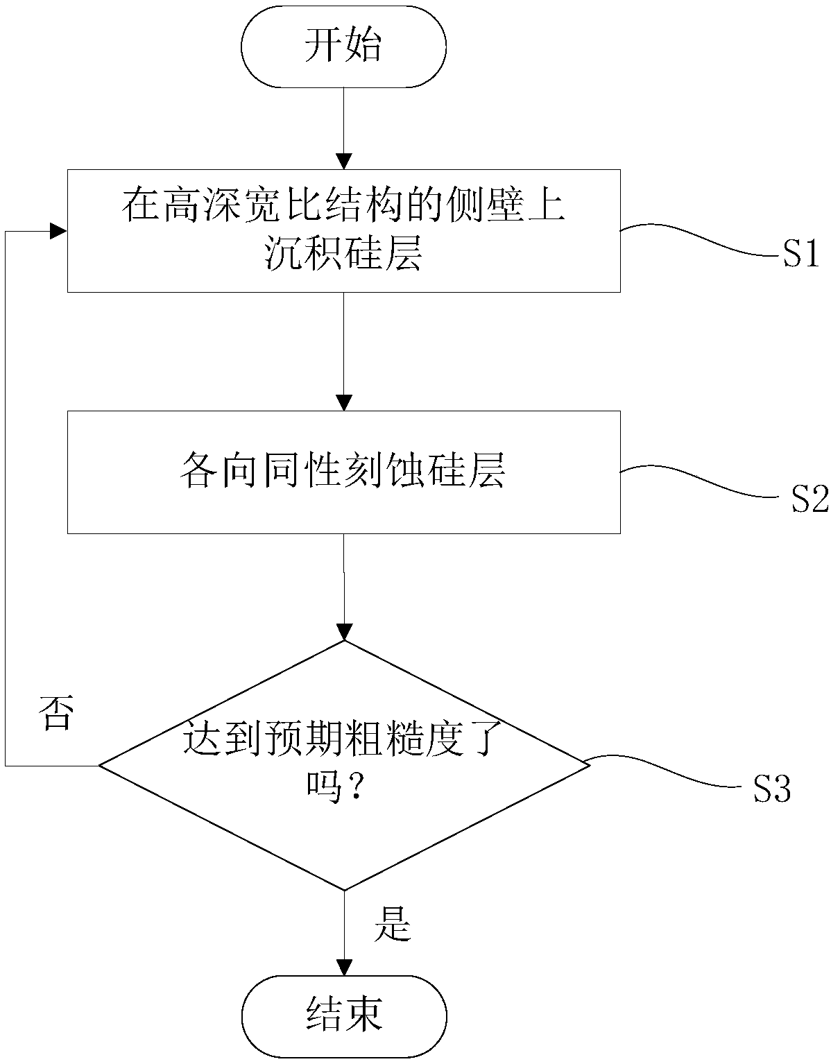
Image

Examples
Embodiment 1
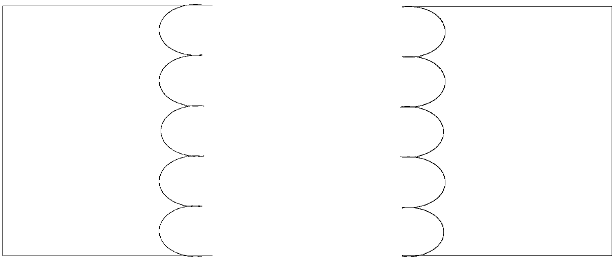
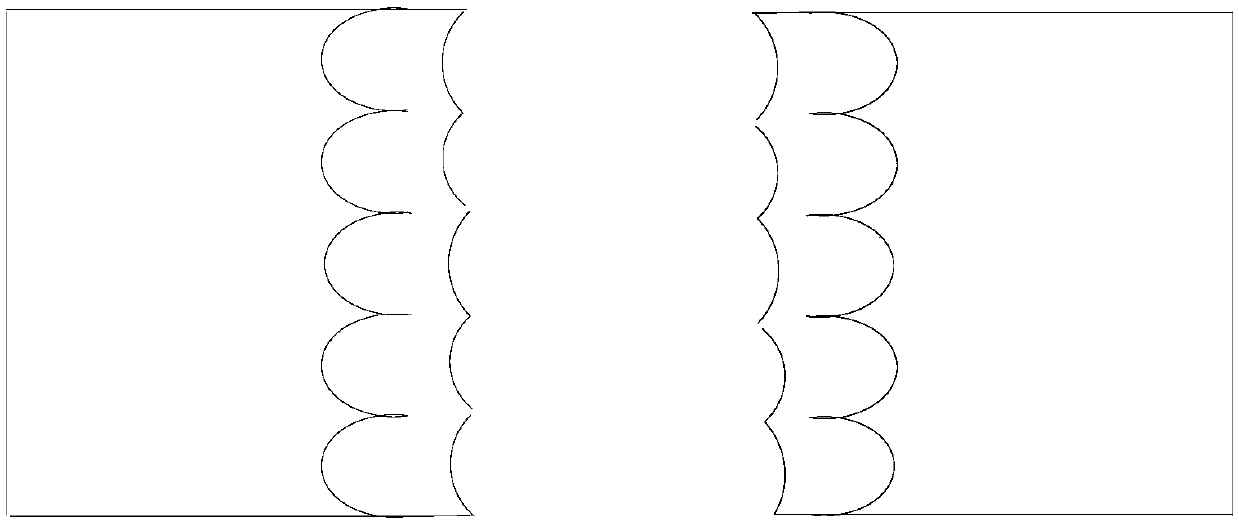
[0038]In this embodiment, a through hole with a diameter of 10 μm and a depth of 200 μm is etched on the silicon substrate by Bosch process, and then the polymer on the side wall is cleaned and removed, and the obtained through hole has a side wall with a roughness of 50 nm. The above-mentioned processes can all adopt conventional processes, which will not be repeated here.
[0039] Next, the method for improving the roughness of the sidewall of the deep silicon etching of the present invention is used to planarize the sidewall of the via hole. First, in the deposition step S1 , 50 nm thick amorphous silicon is deposited on the sidewall of the through hole by using low pressure chemical vapor deposition (LPCVD). Among them, the growth temperature of amorphous silicon is set at 600°C, and the reaction gas is SiH 4 5% SiH 4 The mixed gas with He, the chamber pressure is 50mTorr, and the deposition time is 5min. Then, in the etching step S2, gaseous XeF 2 The silicon is etche...
Embodiment 2
[0043] In this embodiment, a deep groove with a diameter of 10 μm and a depth of 200 μm is etched on a silicon substrate by using the Bosch process, and then the polymer on the sidewall is removed by cleaning, and the roughness of the sidewall of the obtained deep hole is 55 nm. The above-mentioned processes can all adopt conventional processes, which will not be repeated here.
[0044] Next, the sidewall of the deep trench is planarized by using the method for improving the roughness of the sidewall of deep silicon etching of the present invention. First, in the deposition step S1, 55nm thick amorphous silicon is deposited on the sidewall of the deep trench by pulsed plasma enhanced chemical vapor deposition. The growth temperature of amorphous silicon is 350°C, and the reaction gas is SiH 4 5% SiH 4 and a mixed gas of He, the cavity pressure is 50 mTorr, the deposition time is 5 min, the power is 300 W, and the duty cycle of the pulse is 50%. Then, in the etching step S2,...
PUM
| Property | Measurement | Unit |
|---|---|---|
| surface roughness | aaaaa | aaaaa |
Abstract
Description
Claims
Application Information
 - Generate Ideas
- Intellectual Property
- Life Sciences
- Materials
- Tech Scout
- Unparalleled Data Quality
- Higher Quality Content
- 60% Fewer Hallucinations
Browse by: Latest US Patents, China's latest patents, Technical Efficacy Thesaurus, Application Domain, Technology Topic, Popular Technical Reports.
© 2025 PatSnap. All rights reserved.Legal|Privacy policy|Modern Slavery Act Transparency Statement|Sitemap|About US| Contact US: help@patsnap.com